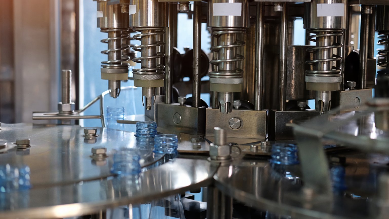
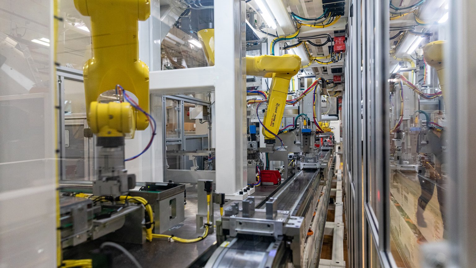
You need machines that can hit increasing production targets and profitably adapt to to changes in demand. Our motion portfolio enables you to do this and more by helping to transform your machines into more productive, intelligent and flexible automation assets. From high-speed packaging lines to advanced material movement and beyond, our motion solutions are designed to elevate what's possible in your designs.
- Overview
- Products
Overview
Key Features
Simpler & More Powerful
Unprecedented Speed & Control
Precision & Performance at Scale
Powerful & Flexible
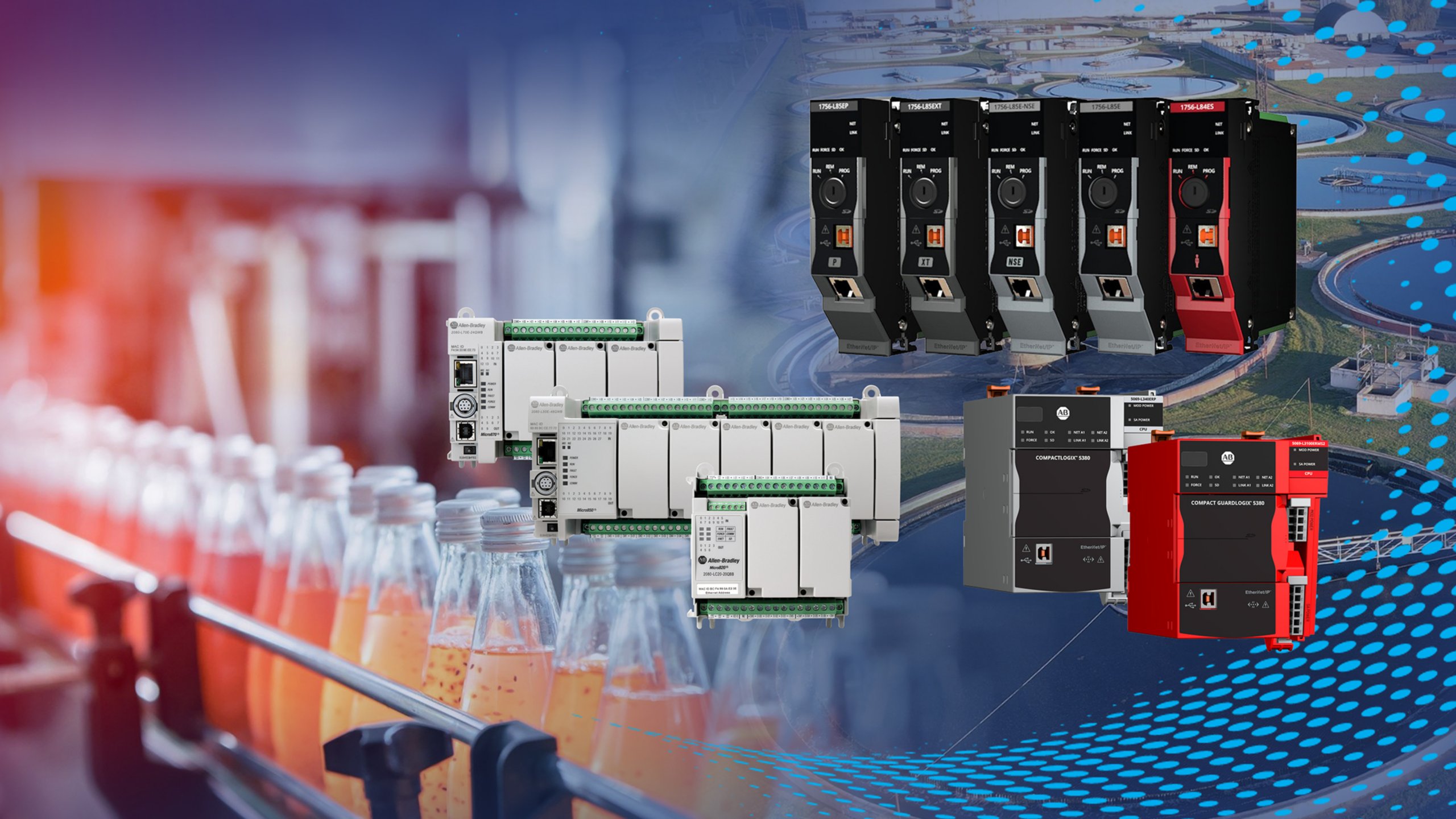
Motion Control
Precise, high‑performance motion to optimize machine speed, accuracy and flexibility.
Complete Your Smart Machine
Build your ideal system using technologies that drive your people and processes forward.

Ready to Deliver Your Next? See What’s New in Motion Control
You need machines that can hit increasing production targets and profitably adapt to changes in demand. Thankfully, you can achieve this and more using our motion control solutions to transform your machines into more productive, intelligent and flexible automation assets. See what’s new in our motion control portfolio and discover how smarter motion technology can help you unlock the full potential of your operations.
What types of applications benefit most from Rockwell Automation motion control?
How does Rockwell Automation simplify commissioning of motion systems?
What communication protocols are supported for motion control?
How can Independent Cart Technology improve machine throughput?
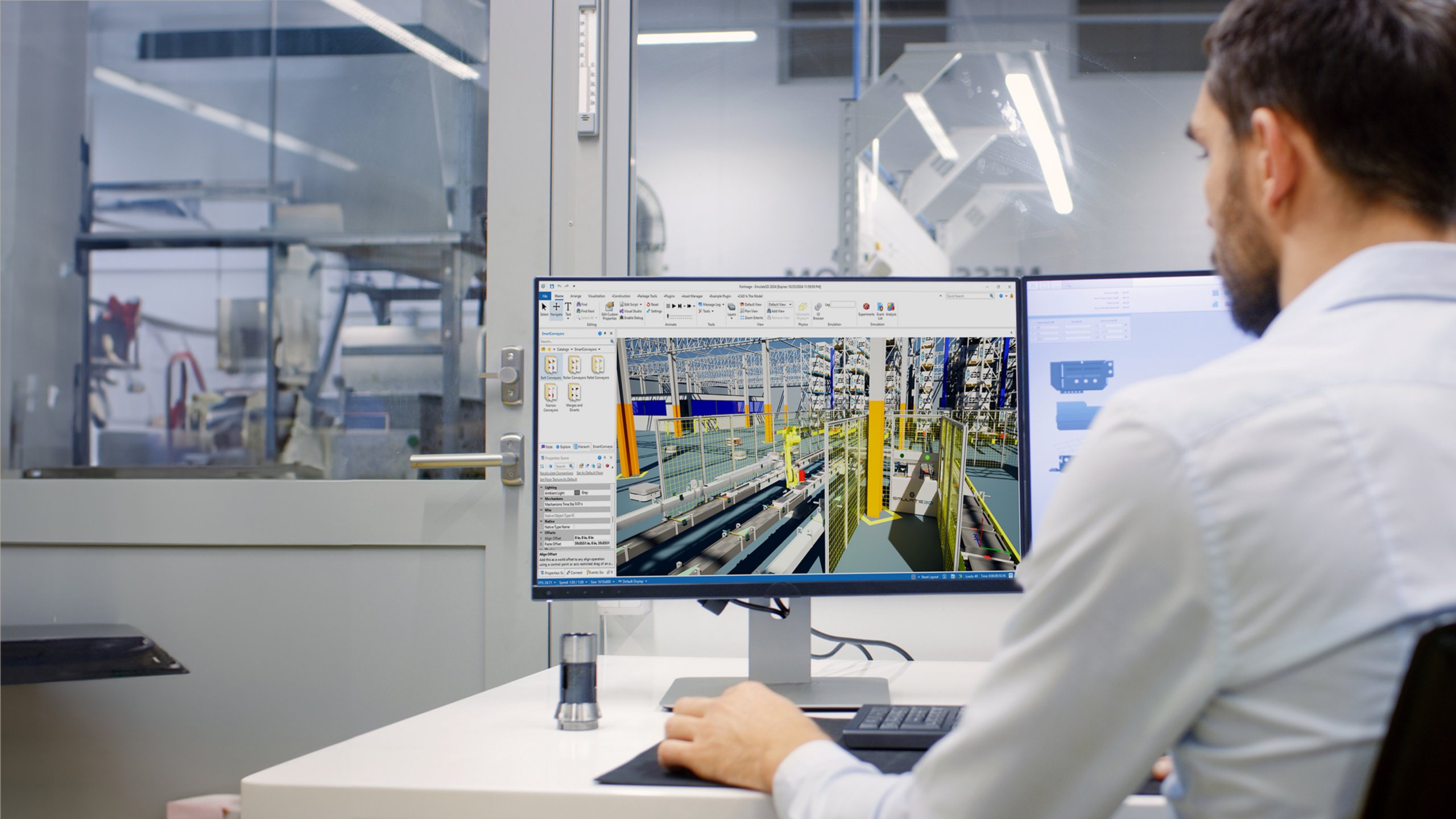
What tools support digital engineering for motion systems?
Simplify Your Processes with the Right Resources and Support
Technical Documentation Center
Technical specifications, manuals and installation instructions.
Remote Technical Support
Real-time online and phone support from product specialists.
PartnerNetwork
A team of engineering specialists and suppliers that are leaders in the industry.
Literature Library
Publications that support Rockwell Automation, FactoryTalk and Allen‑Bradley products, services and solutions.
Knowledgebase
A database of questions and answers on a variety of products and technologies.
Connect with a Rockwell Automation Expert Today
We help you launch faster, reduce risk, and maximize results. Let’s build smarter, together.
Based on Your Activity
Products
Showing
1
-
1
of
0
Results
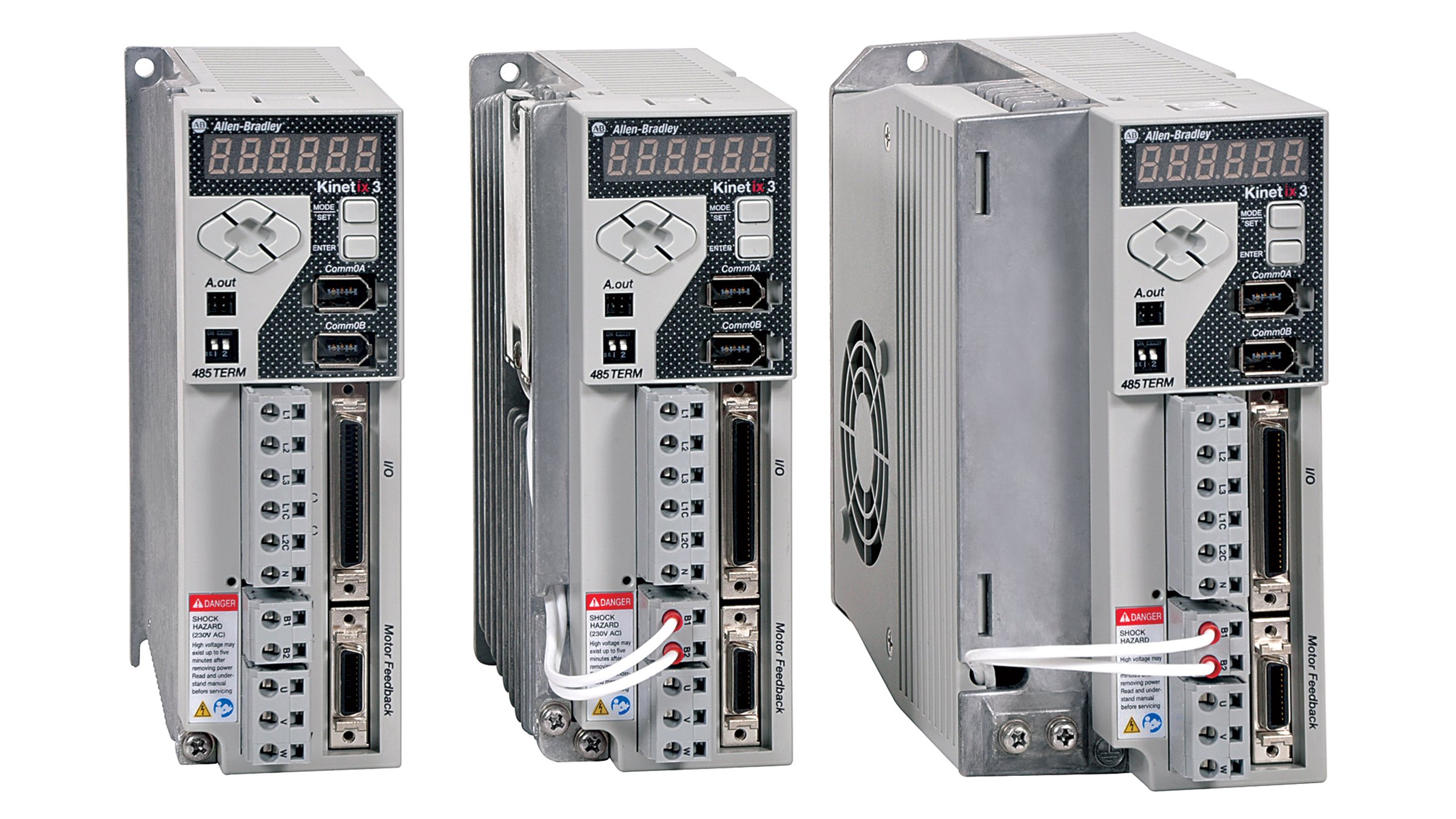
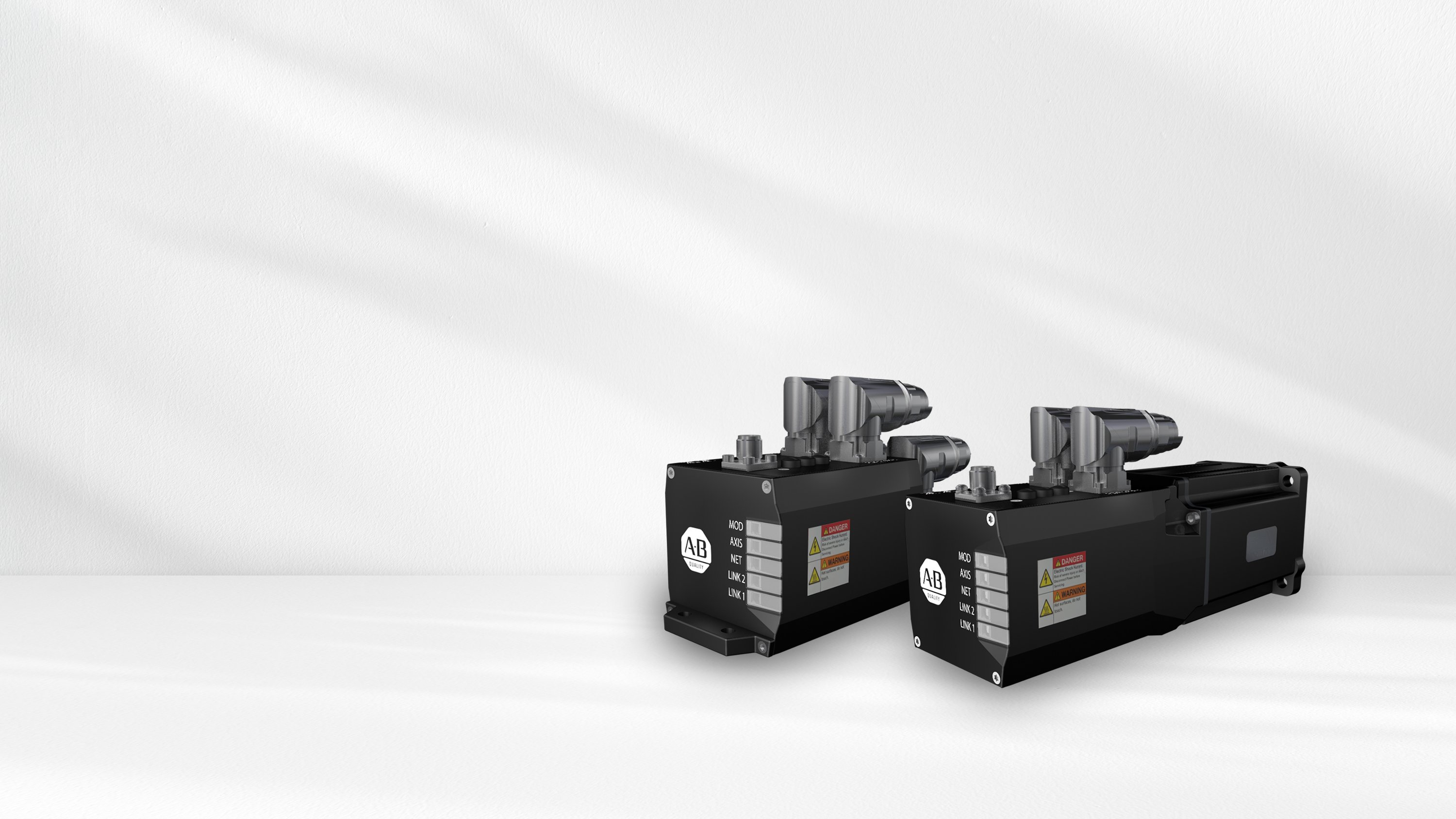
ArmorKinetix Distributed Servo Drives
Realize more simplified, energy-efficient machines and unleash the power of decentralized motion control with ArmorKinetix distributed servo drives.
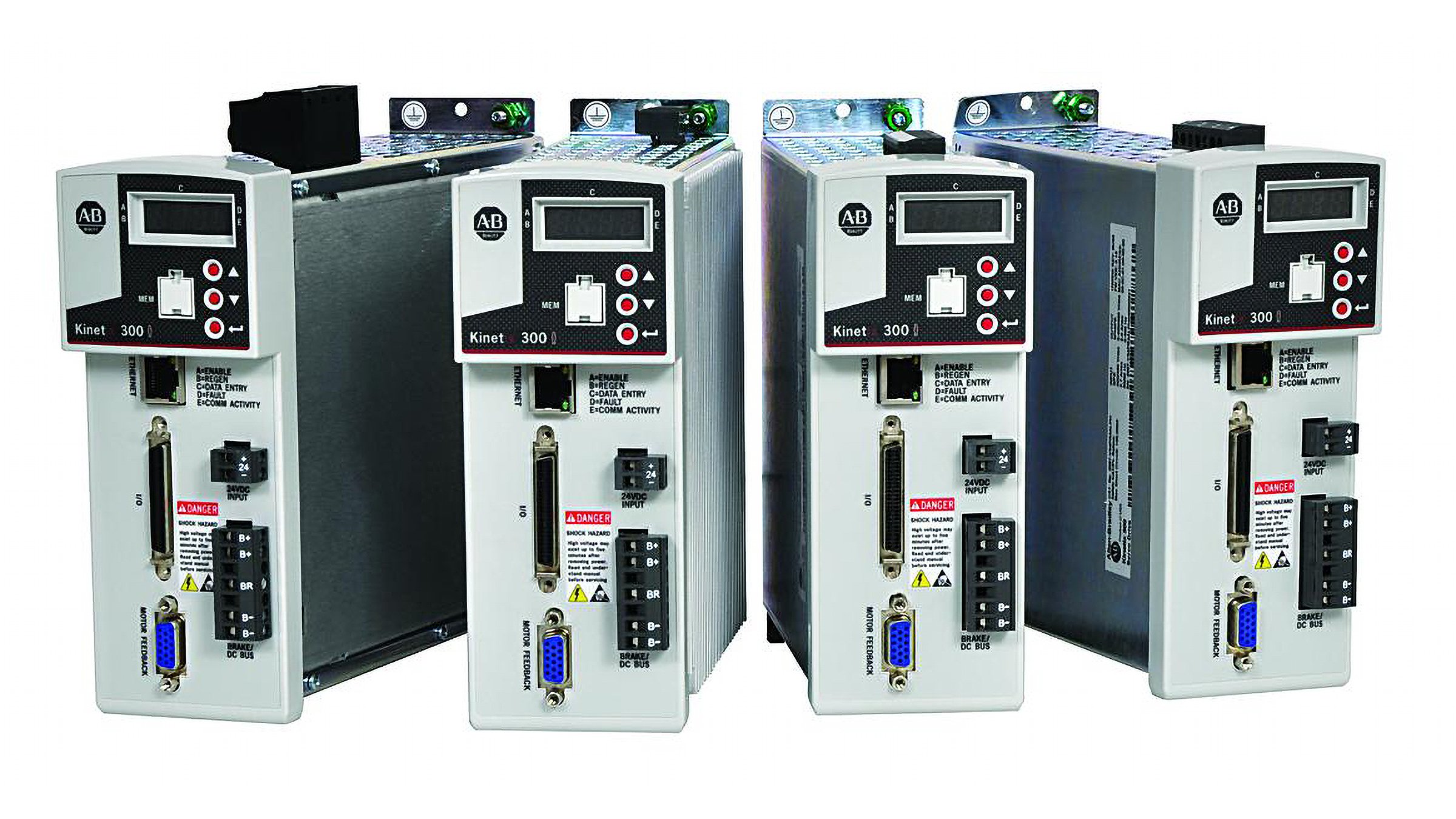
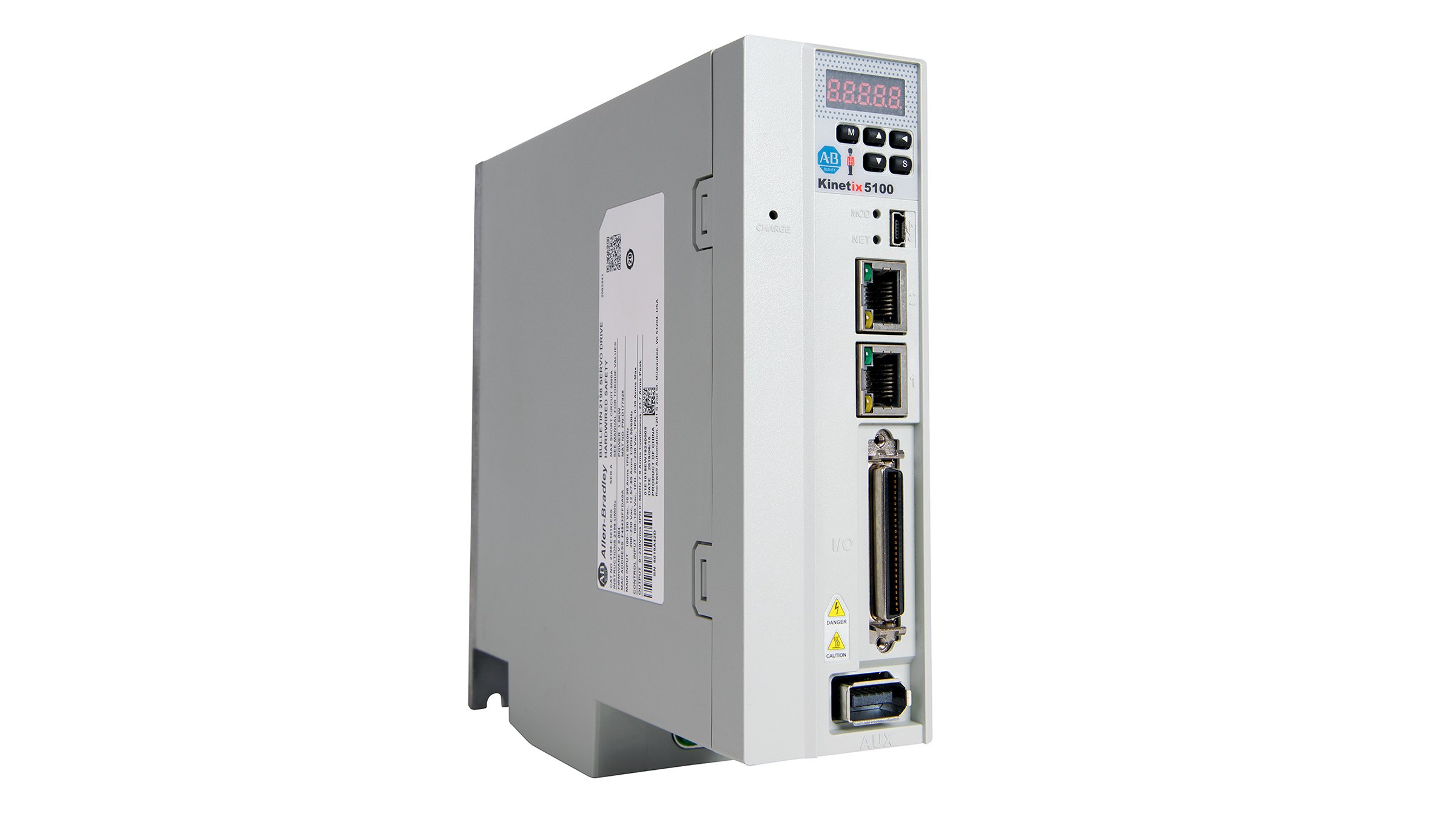
Kinetix 5100 Servo Drives
The versatile Kinetix 5100 servo drives elevate the performance and scalability of your small- to medium-sized machines.
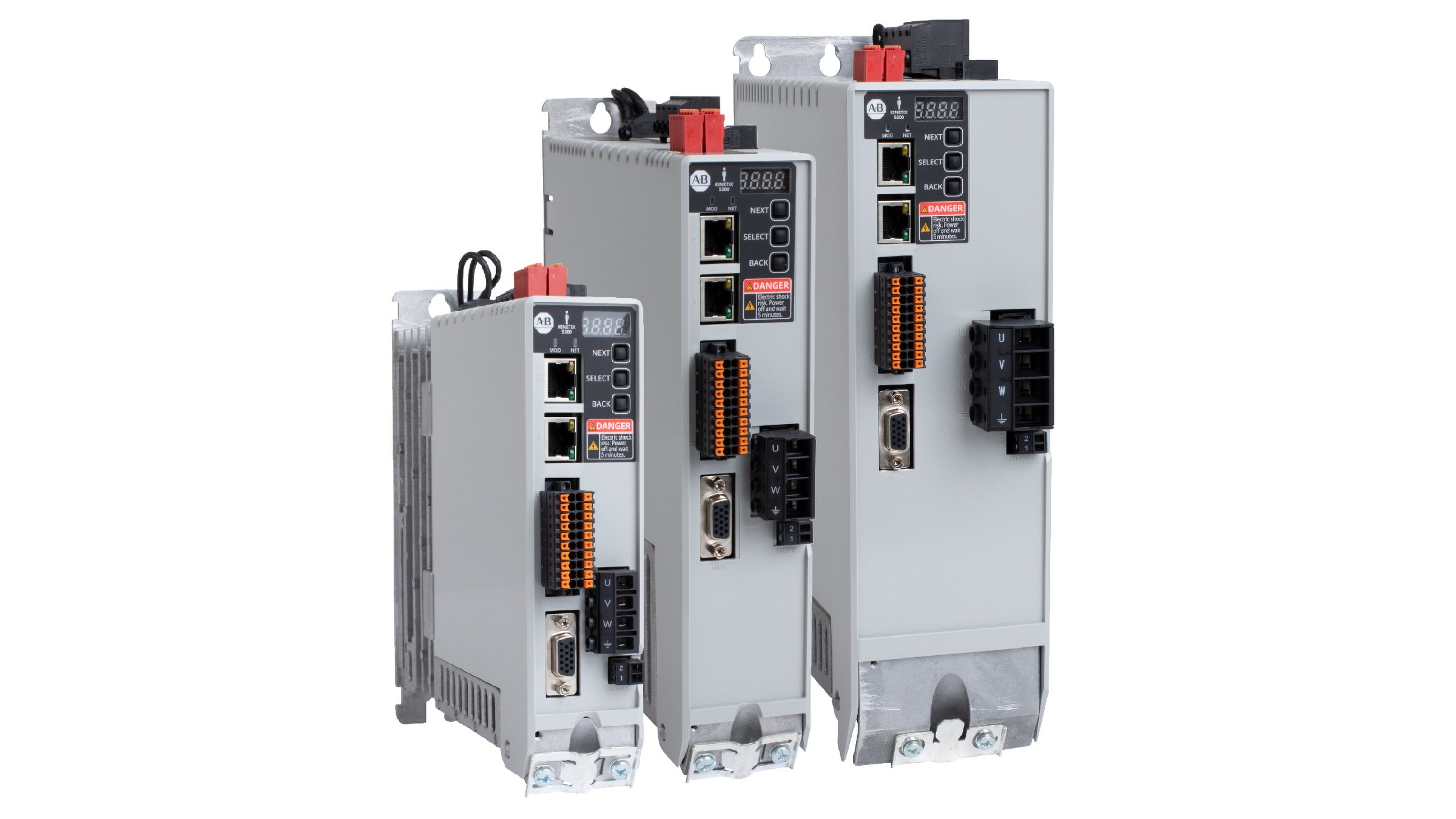
Kinetix 5300 Servo Drives
These single-axis EtherNet/IP servo drives provide design flexibility in a streamlined offering to cover your essential machine-building needs.
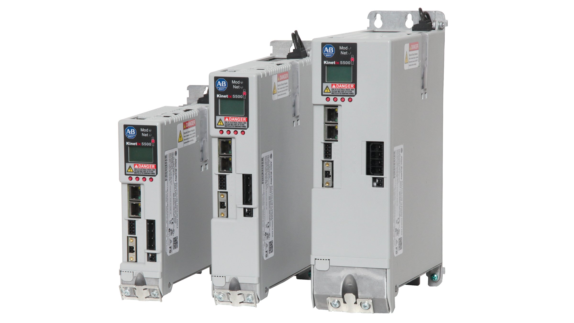
Kinetix 5500 Servo Drives
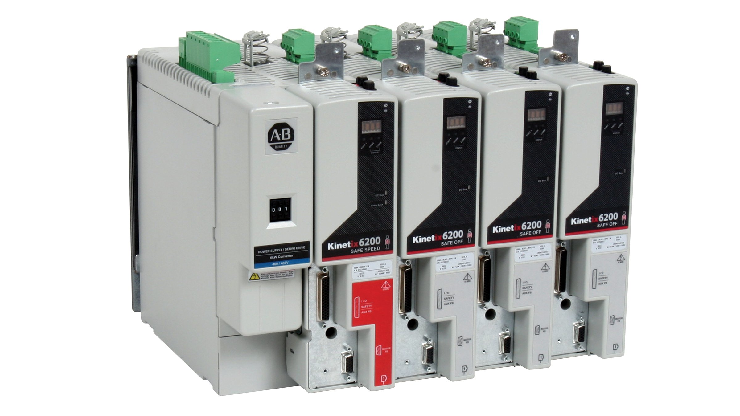
Our Kinetix 5500 Servo Drives provide versatile EtherNet/IP motion solutions that help to simplify designs and create agile, cost-effective solutions.
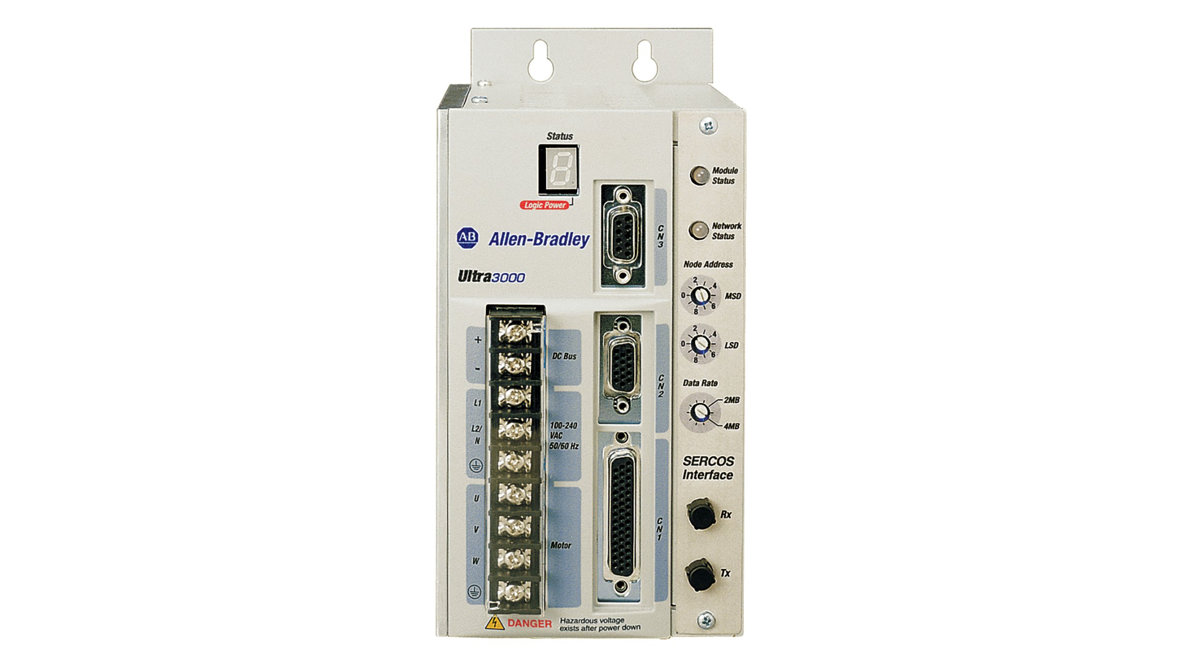
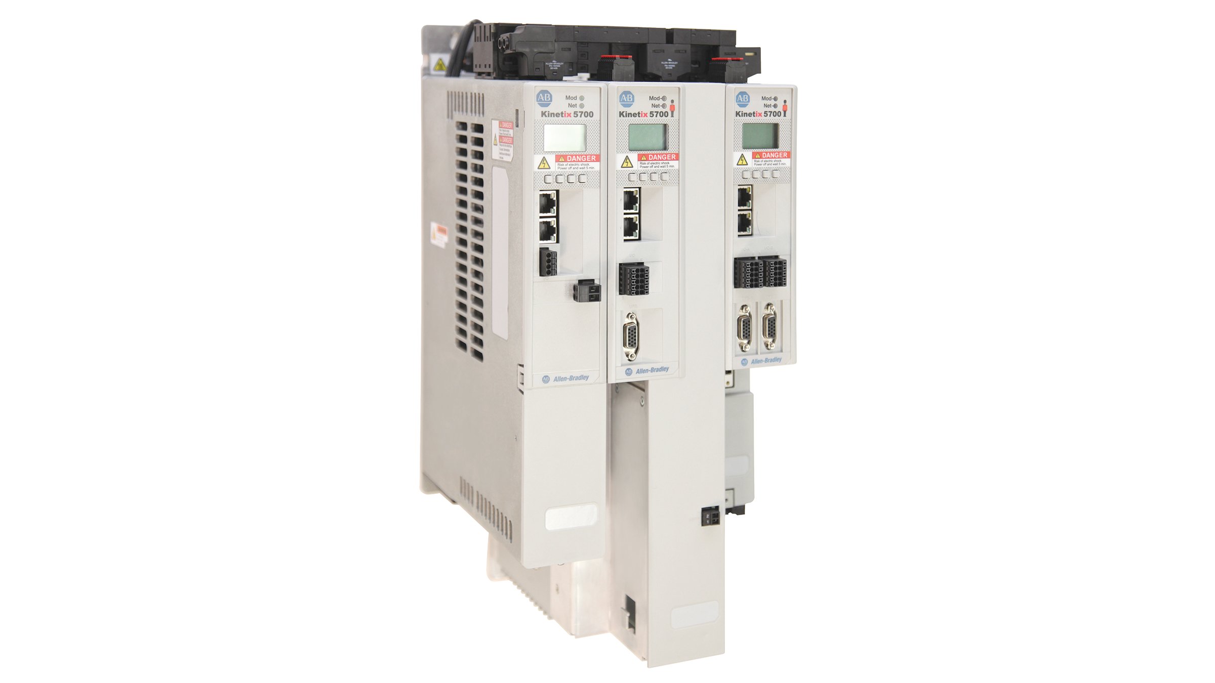
Kinetix 5700 Servo Drives
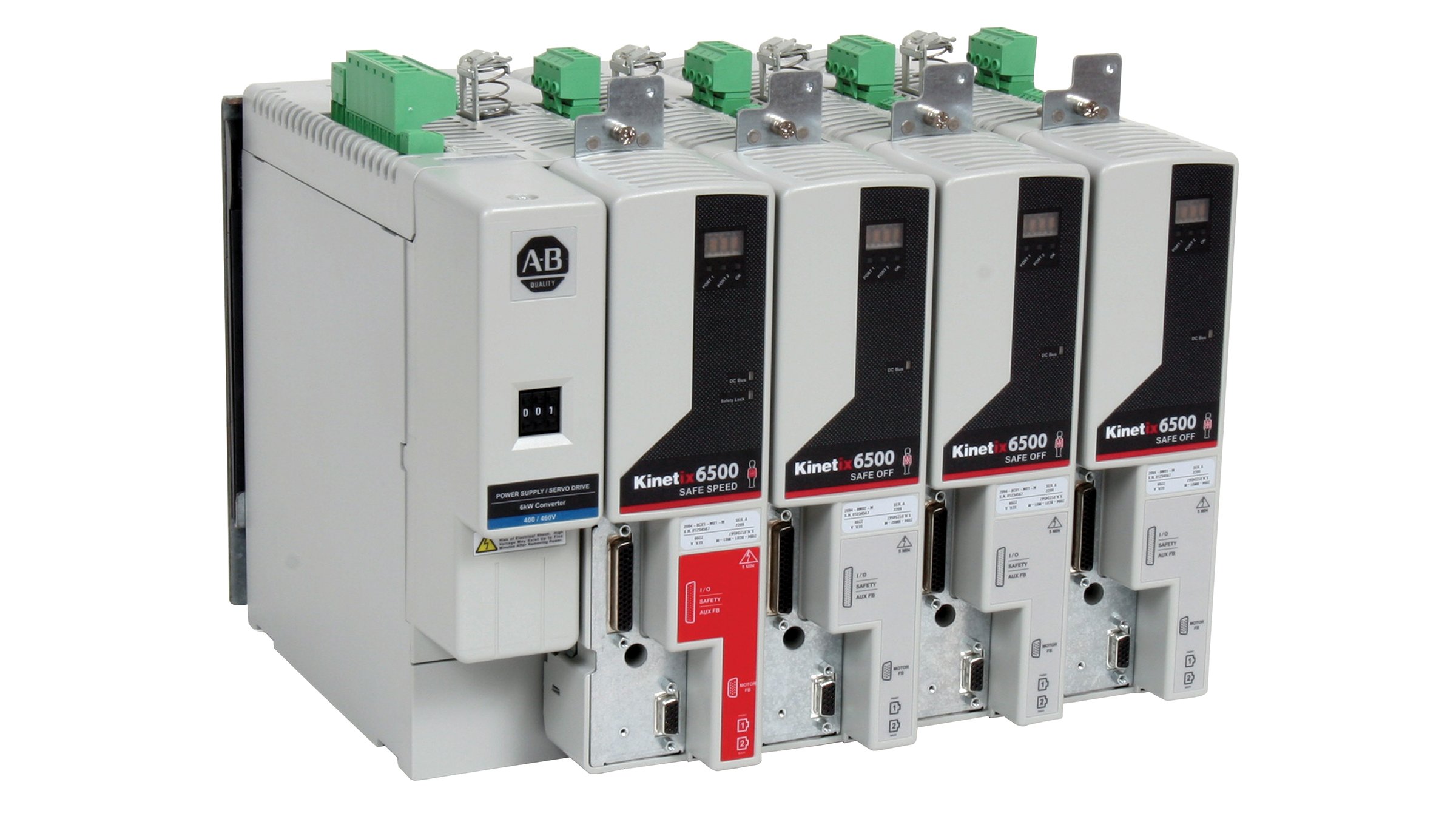
Our Kinetix 5700 Servo Drives offer the simplicity, power and space savings to help optimize motion performance and maximize machine value.
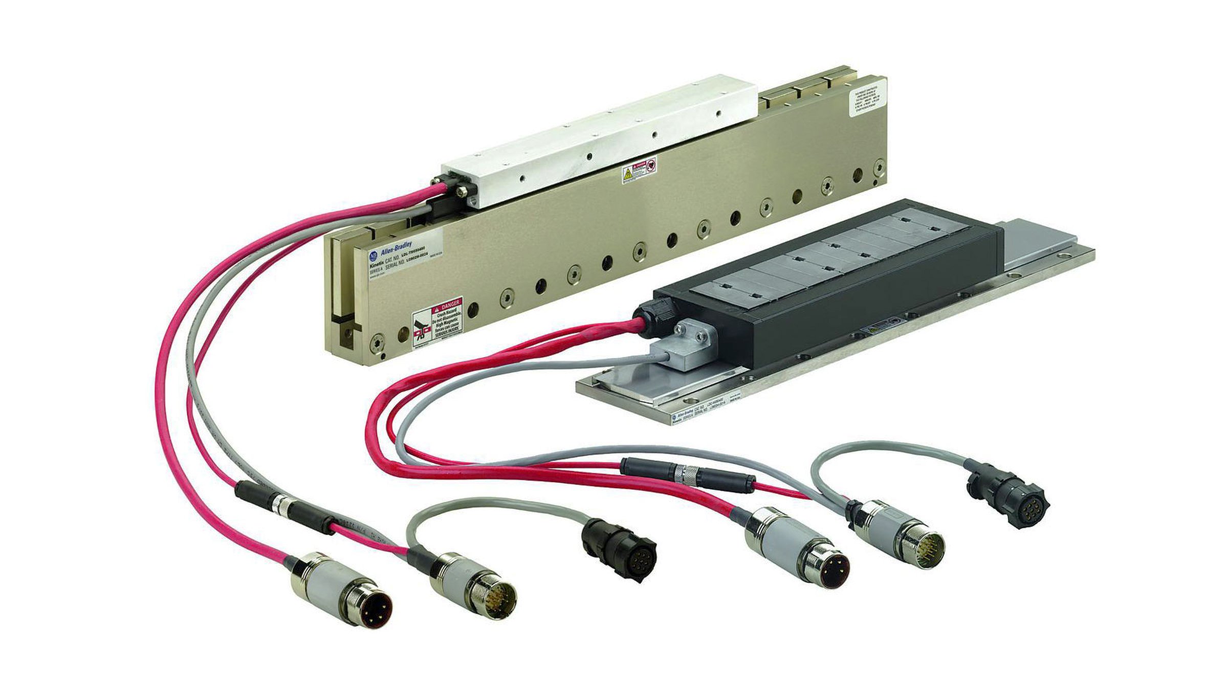
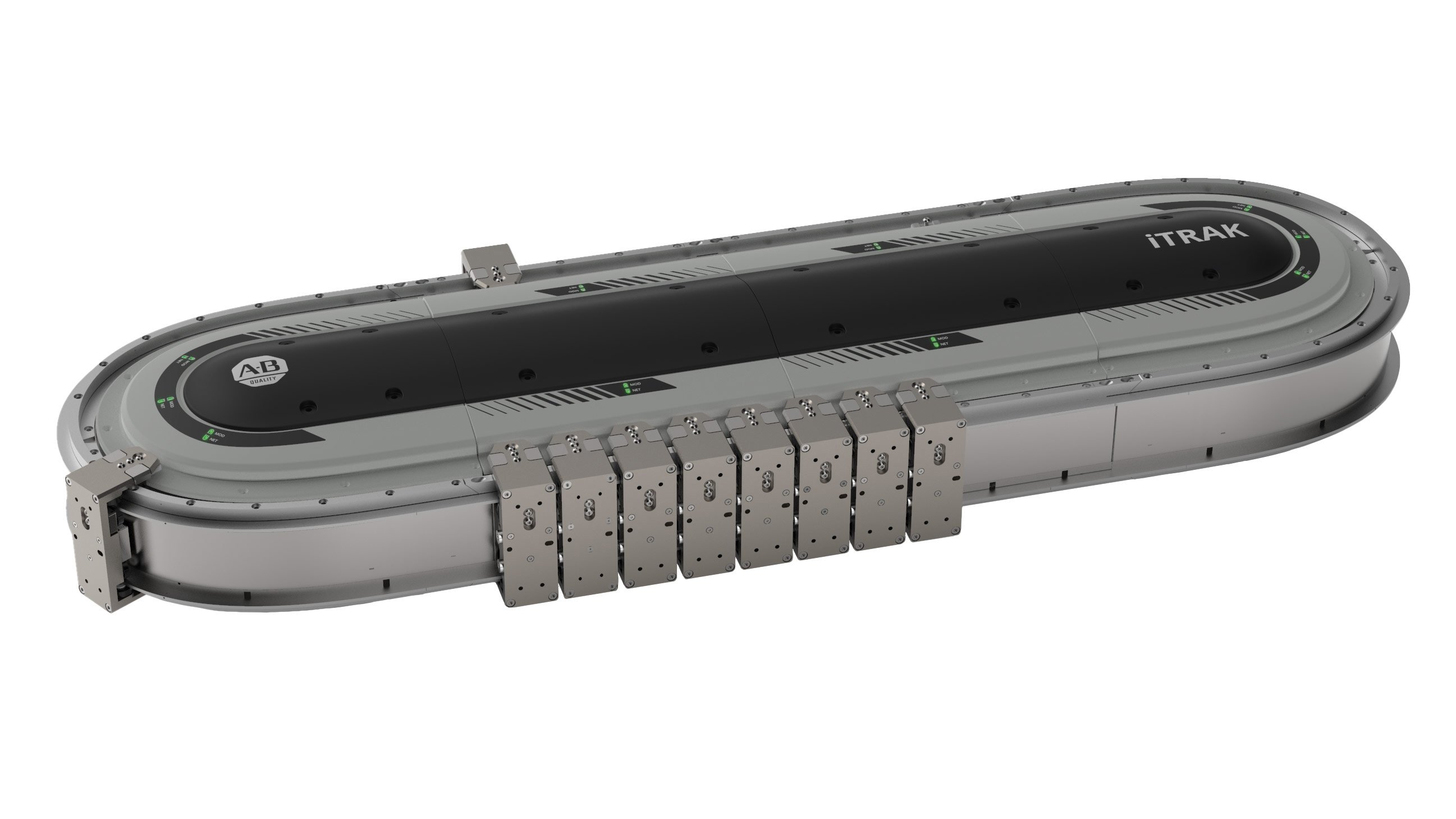
iTRAK 5730 Intelligent Track System
Remove bottlenecks and boost overall productivity with a faster, smarter and more flexible way to move goods within your machines.
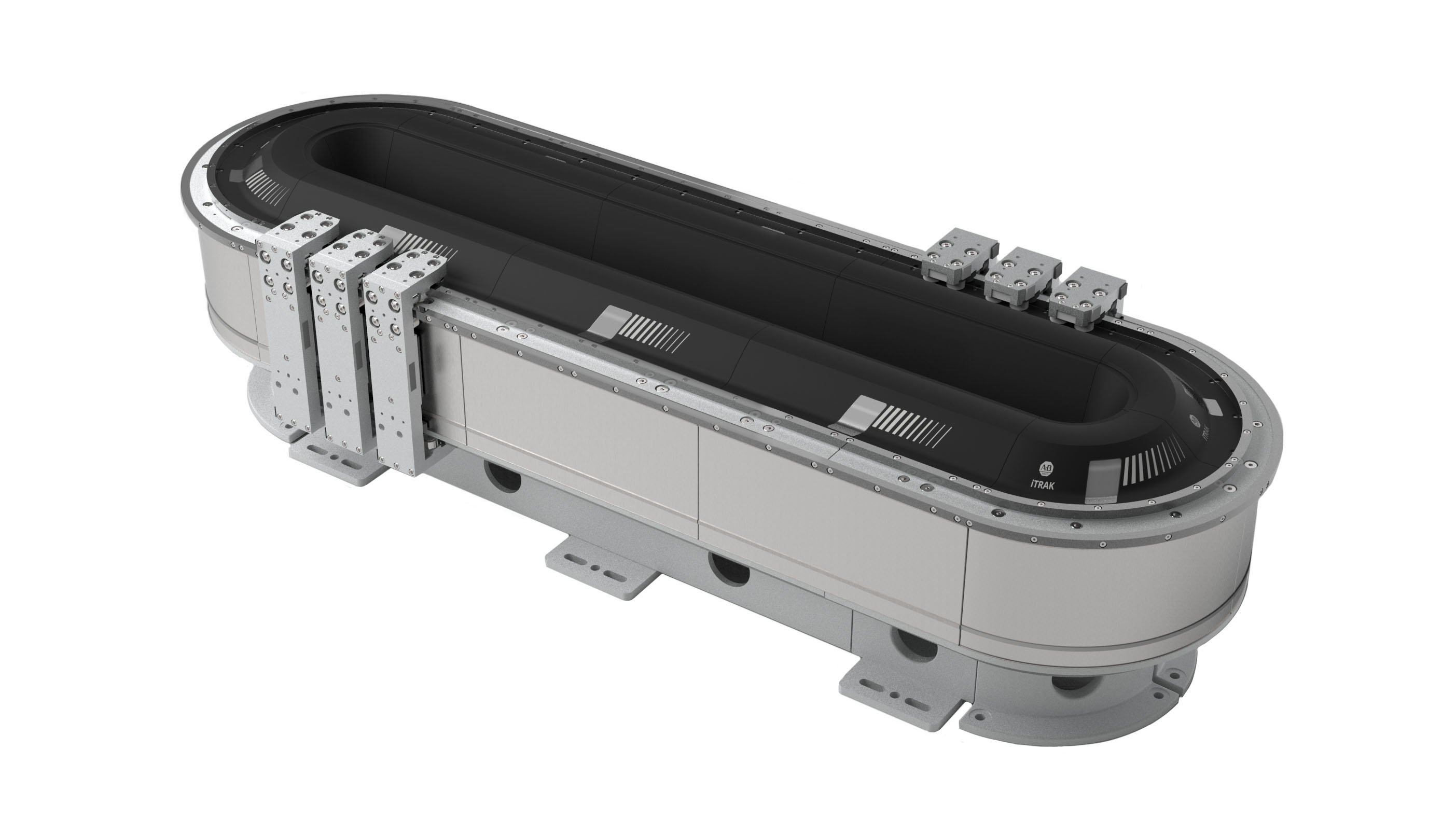
iTRAK 5750 Intelligent Track System
Our iTRAK 5750 Intelligent Track System enables you to redefine your machine productivity and move higher payloads with more flexibility and control.
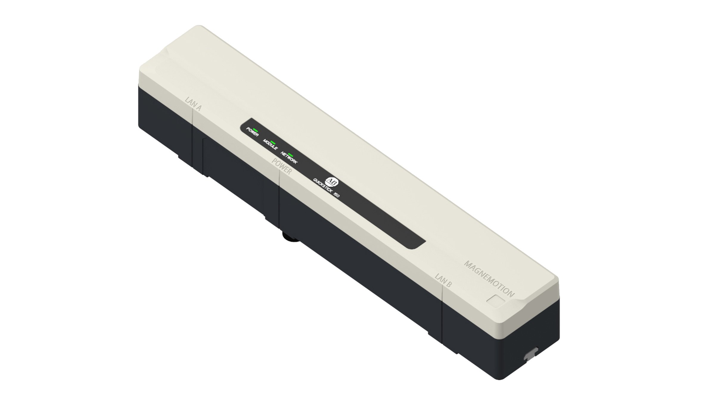
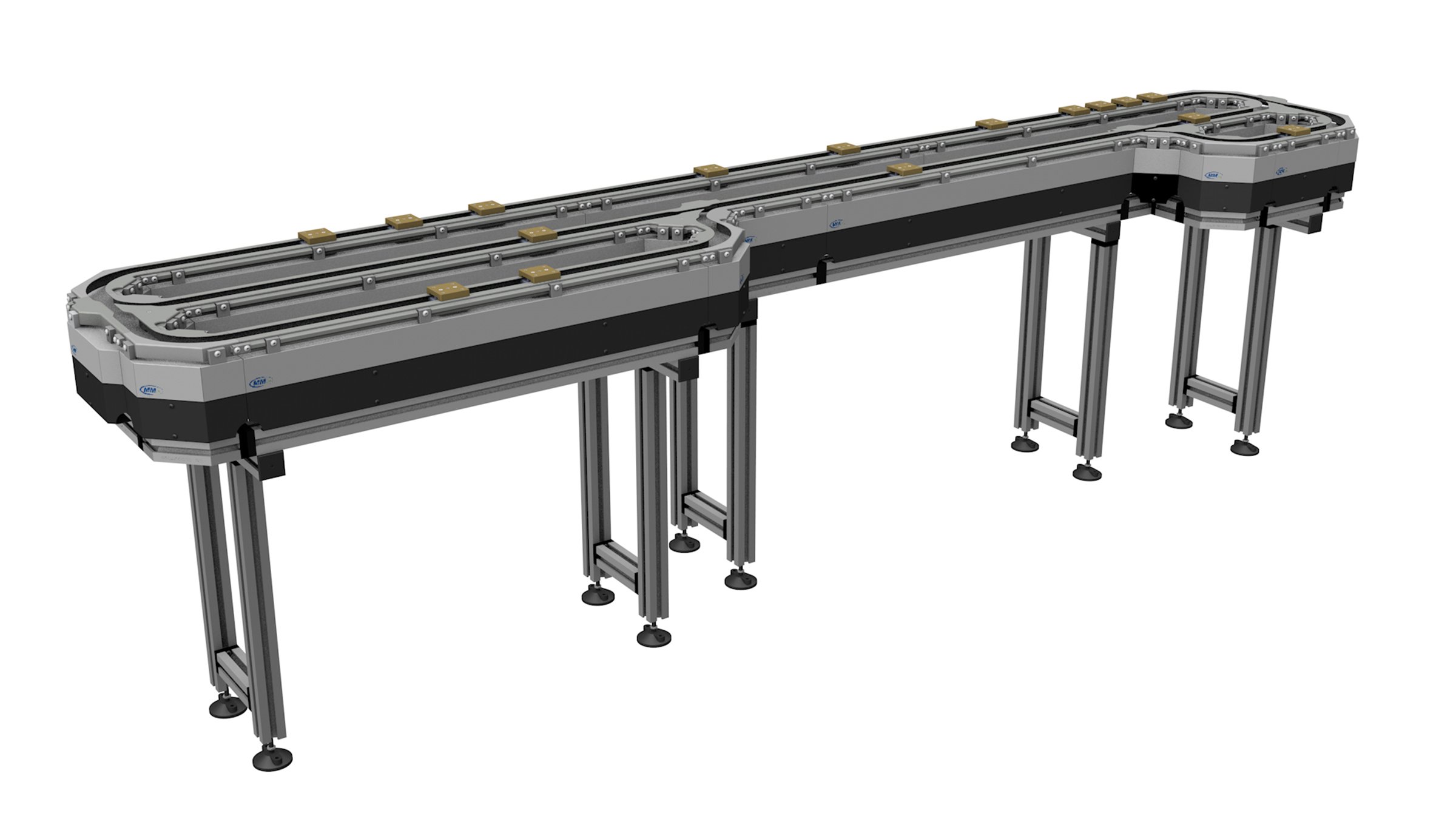
QuickStick 150 Intelligent Conveyor System
Our OuickStick® 150 Intelligent Conveyor System enables you to get more from your operations with faster, cleaner and more efficient transportation of goods.
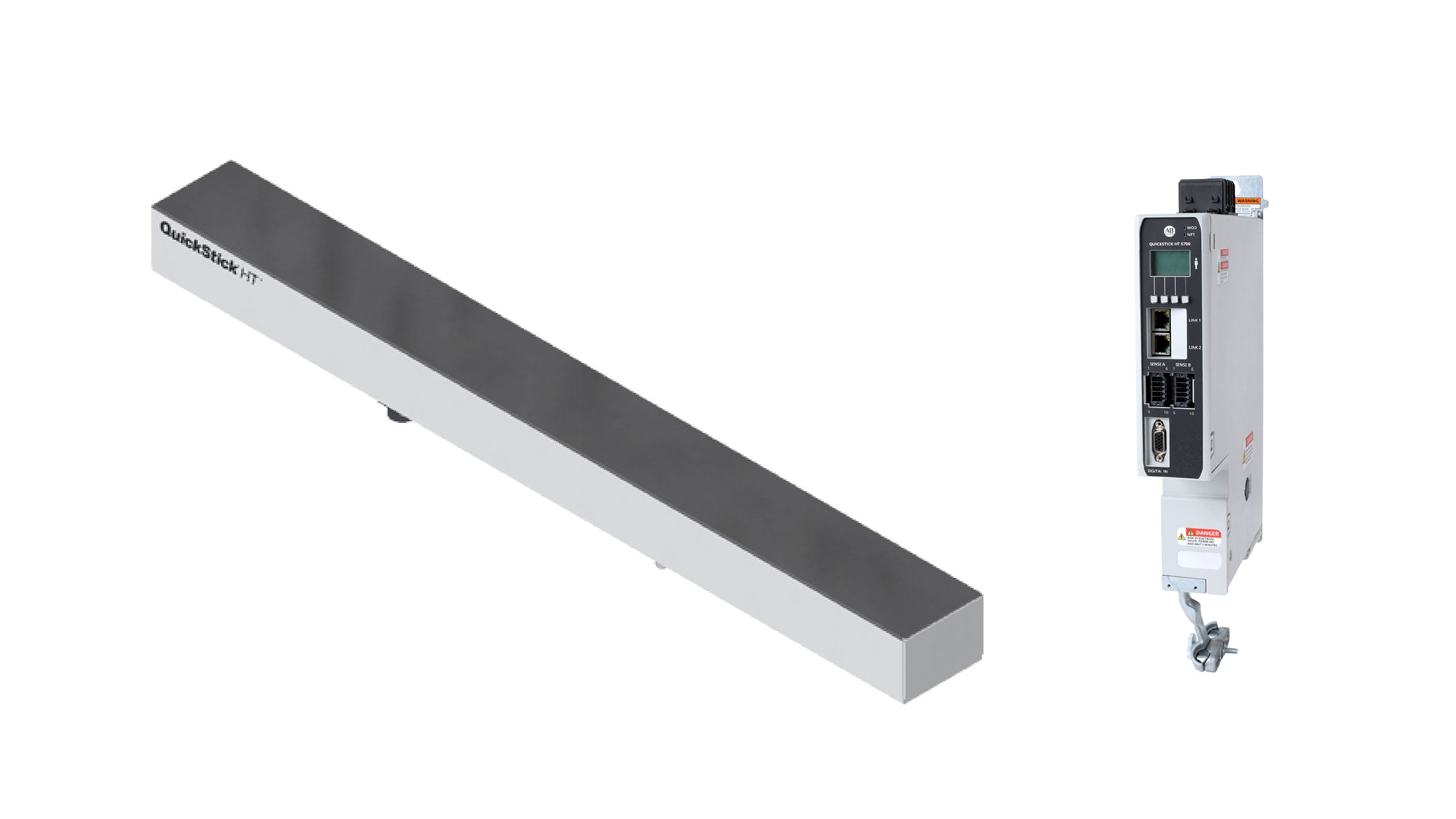
QuickStick HT Intelligent Conveyor System
Unlock more flexible and productive processes using our QuickStick® HT Intelligent Conveyor System to move heavy loads up to thousands of kilograms.
MagneMover LITE Intelligent Conveyor System
Move small to medium loads faster and more efficiently using our MagneMover LITE Intelligent Conveyor System.
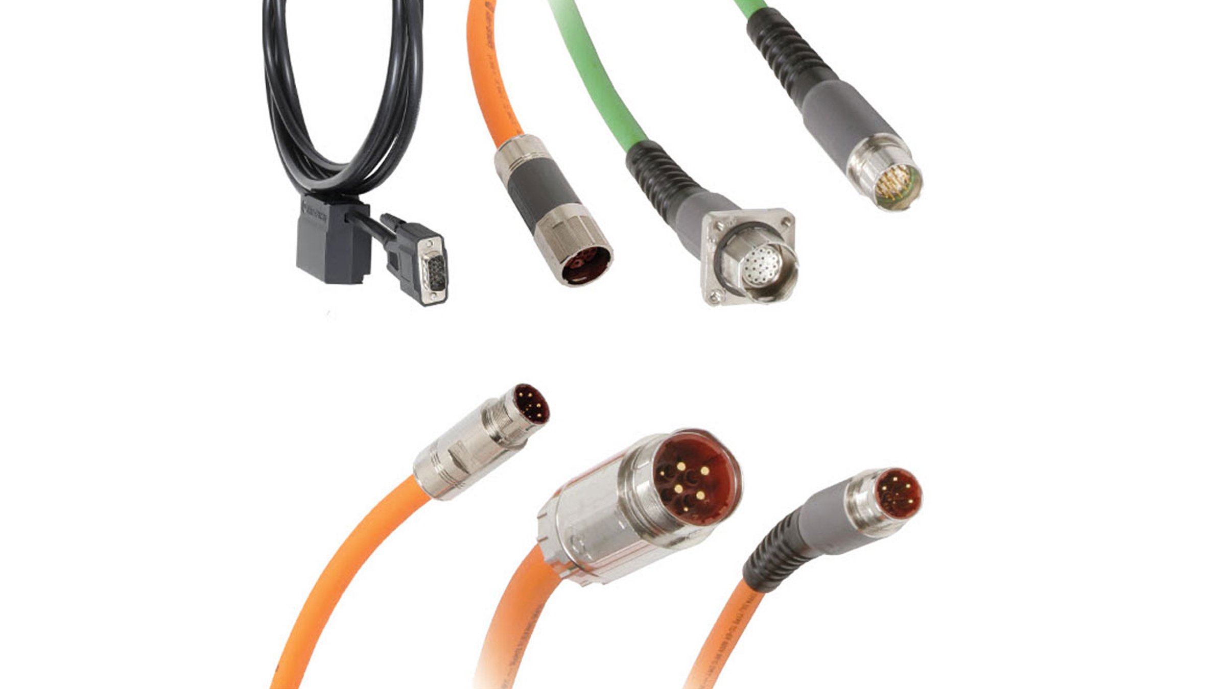
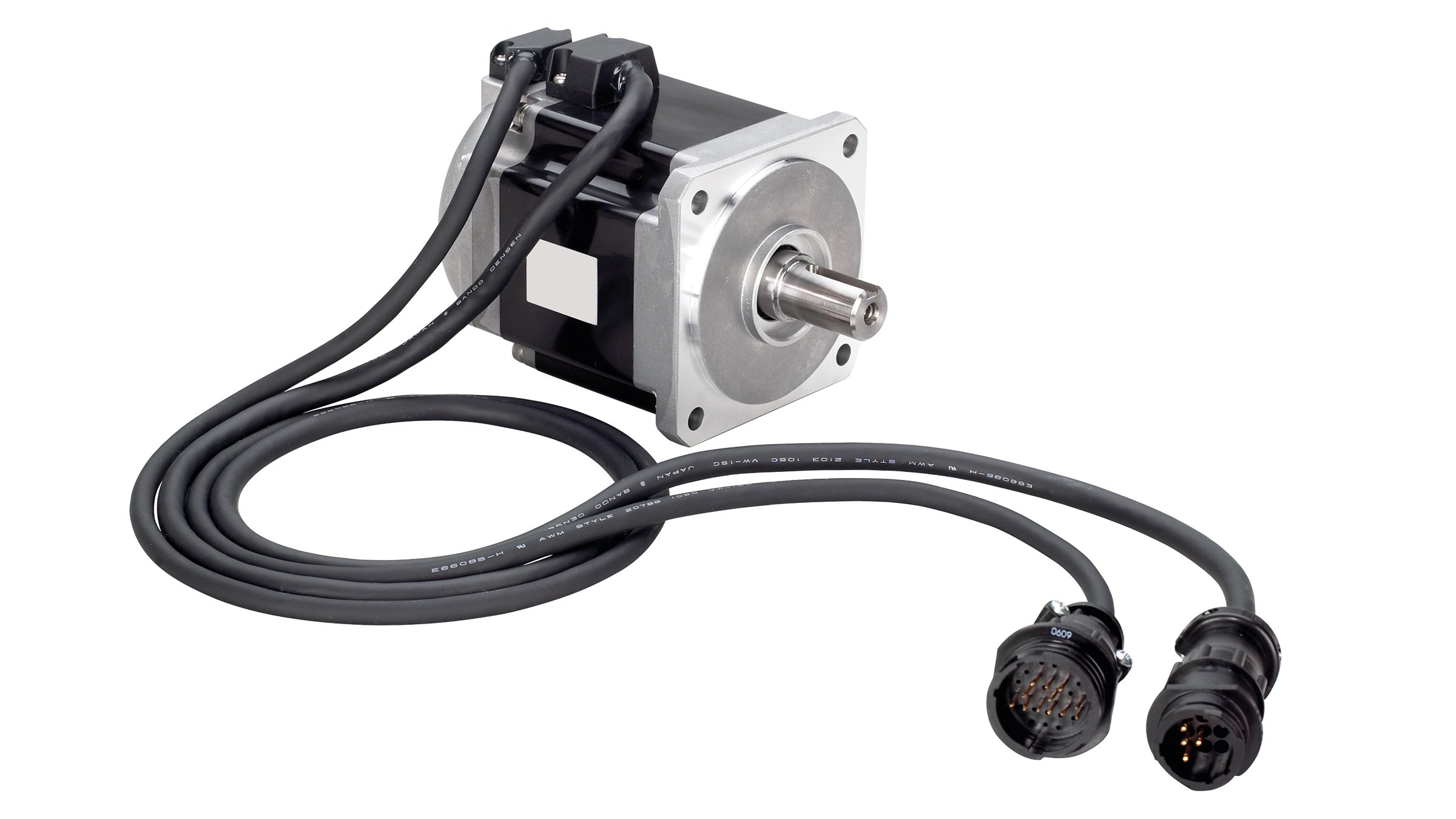
Kinetix Cables
Securely connect your servo motors and actuators using our family of standard and continuous flexing cables.
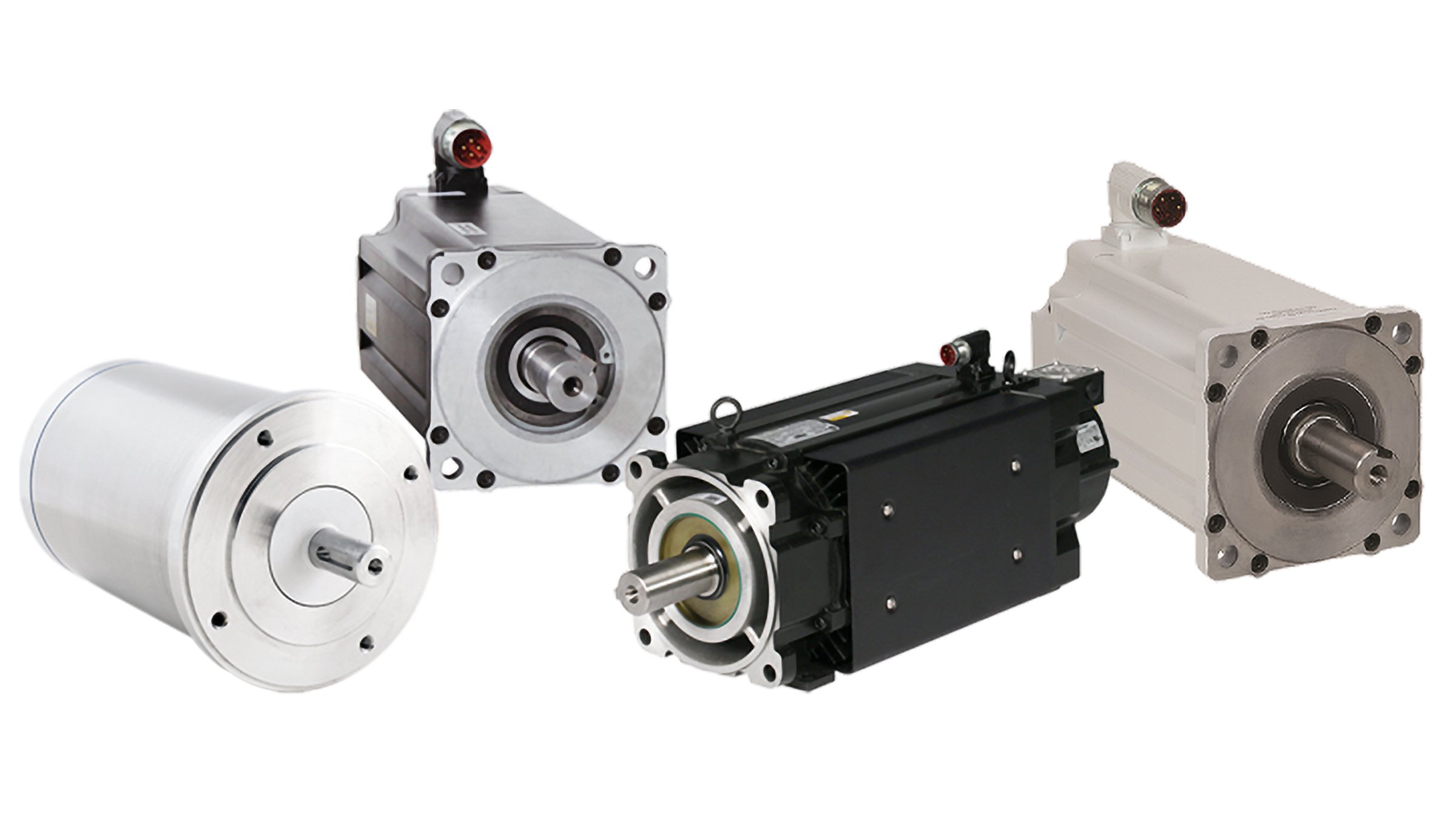
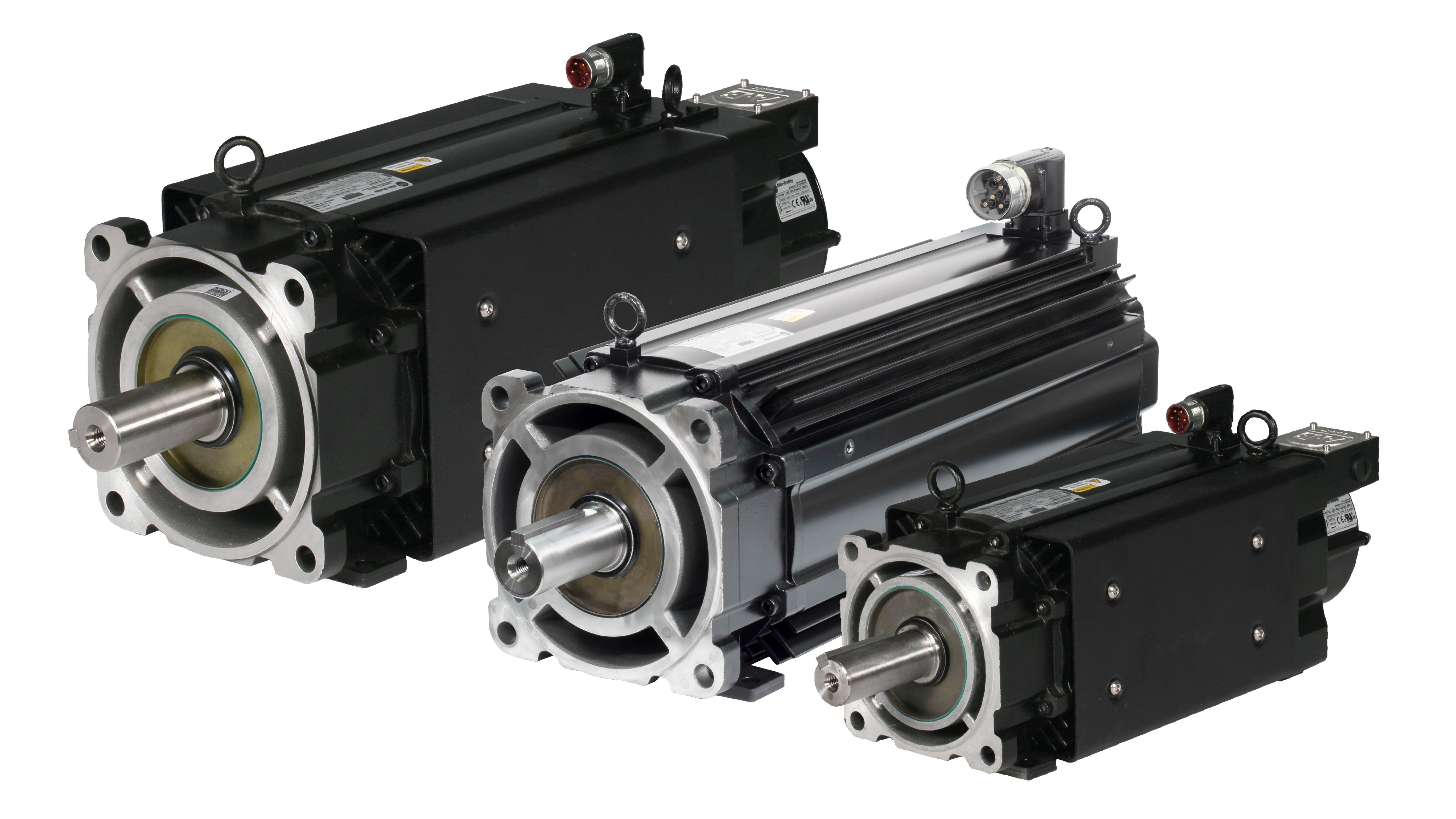
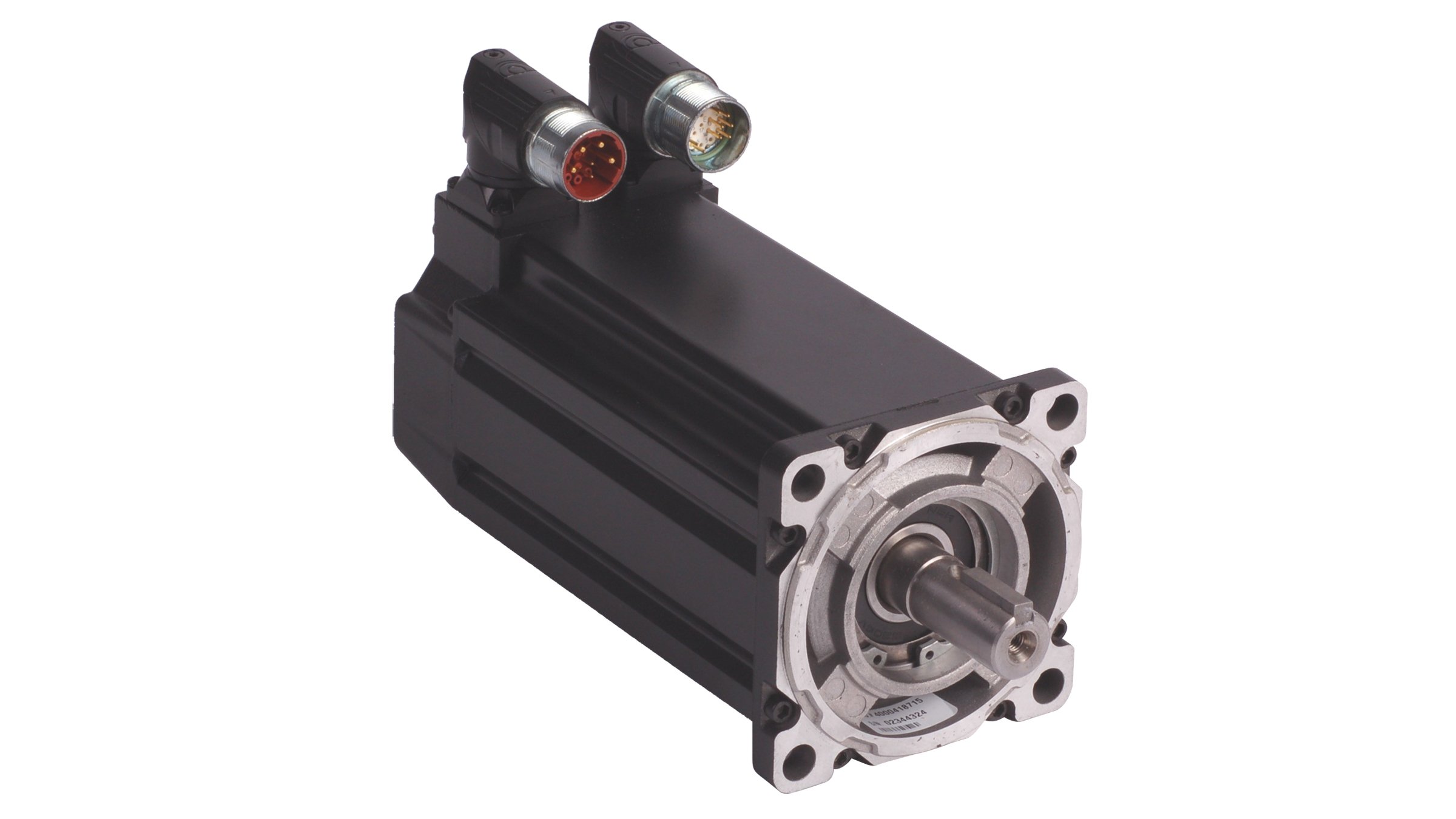
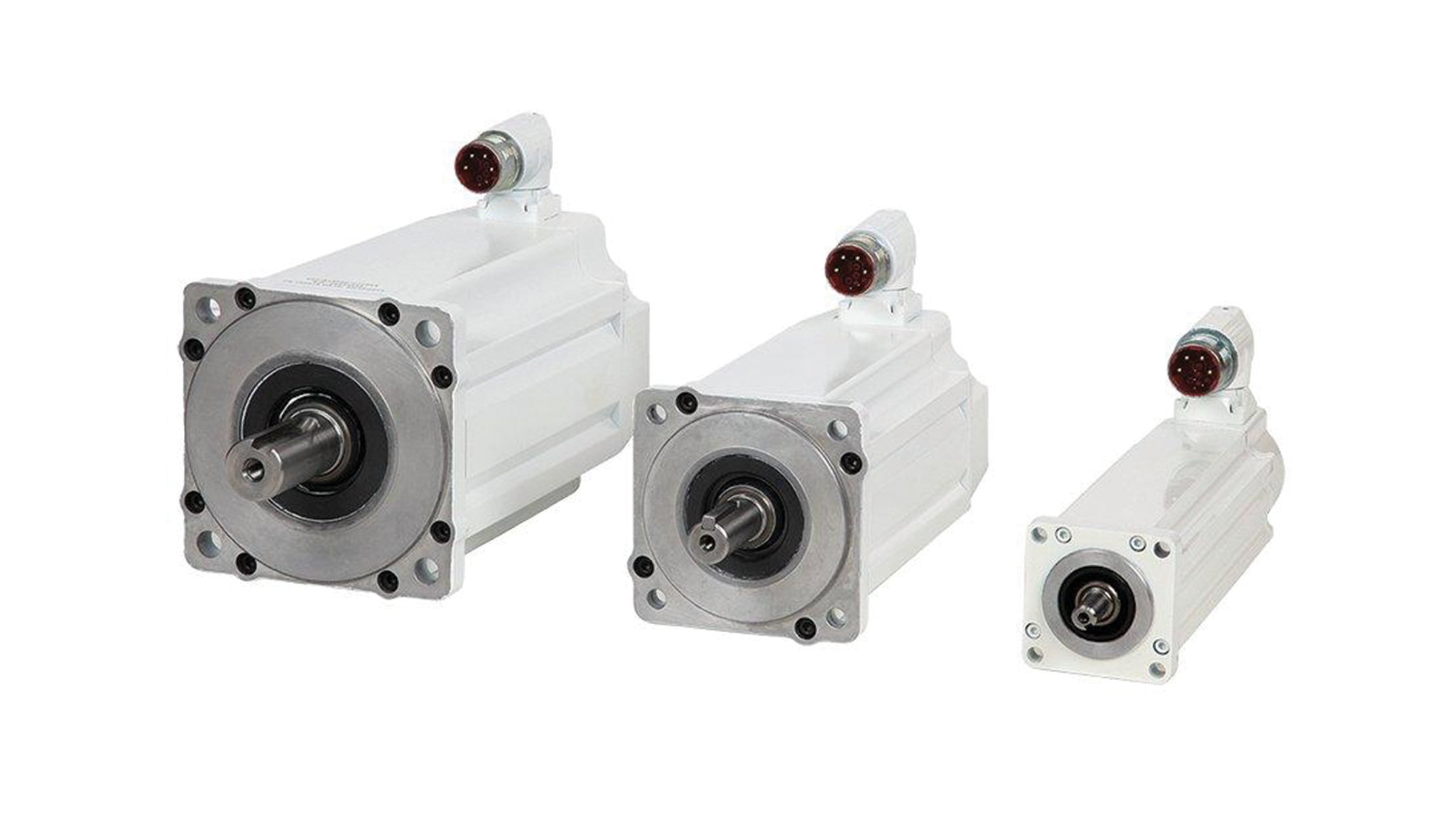
Kinetix VP Servo Motors
These motors provide smooth, integrated motion control over your EtherNet/IP network and are optimized for the Kinetix 5500 and 5700 servo drives.
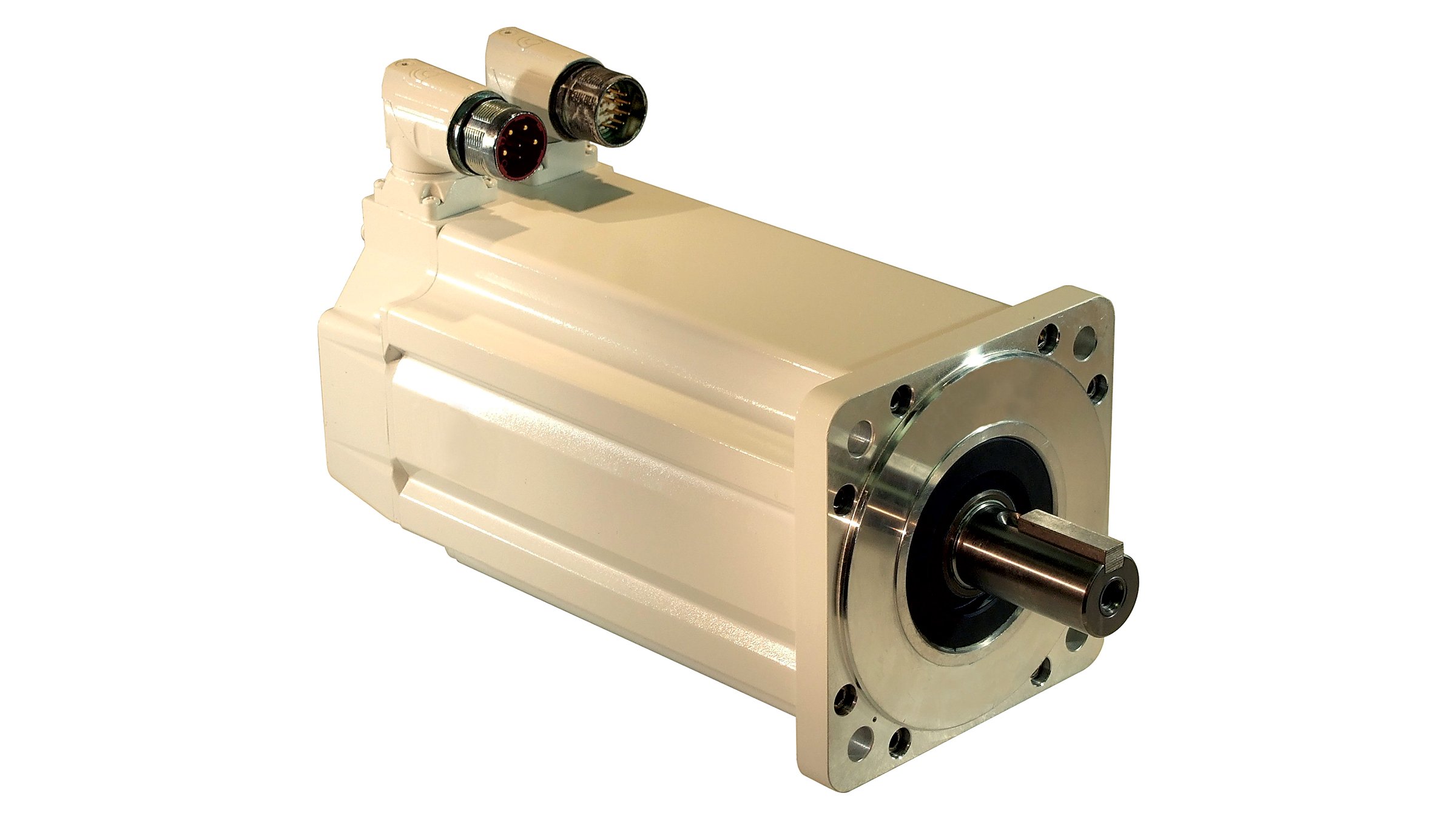
Kinetix VPL Low-inertia Servo Motors
Maximize your machine potential using our Kinetix® VPL Low-inertia Servo Motors to move loads with quick accelerations and exceptional precision.
Kinetix VPC Continuous-duty Servo Motors
Select these motors to optimize your continuous-duty applications and deliver more efficiency and higher torque at higher speeds.
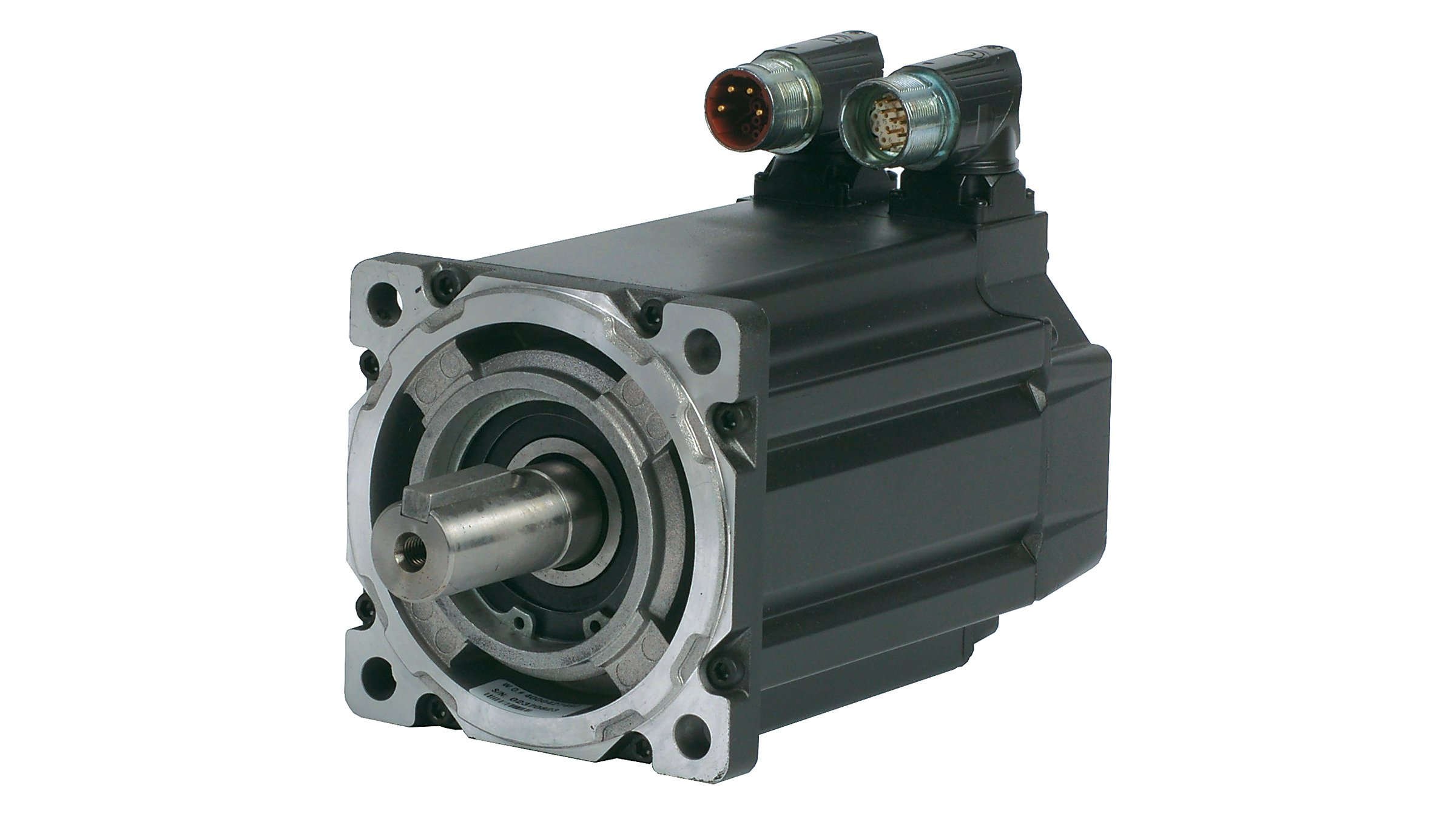
Kinetix MPL Low-inertia Servo Motors
Increase your competitive advantage with these high-output brushless motors that deliver higher torque with a reduced footprint.
Kinetix MPM Medium-inertia Servo Motors
These motors feature a compact, power-dense design and high-resolution absolute encoder to maximize the potential in your processes.
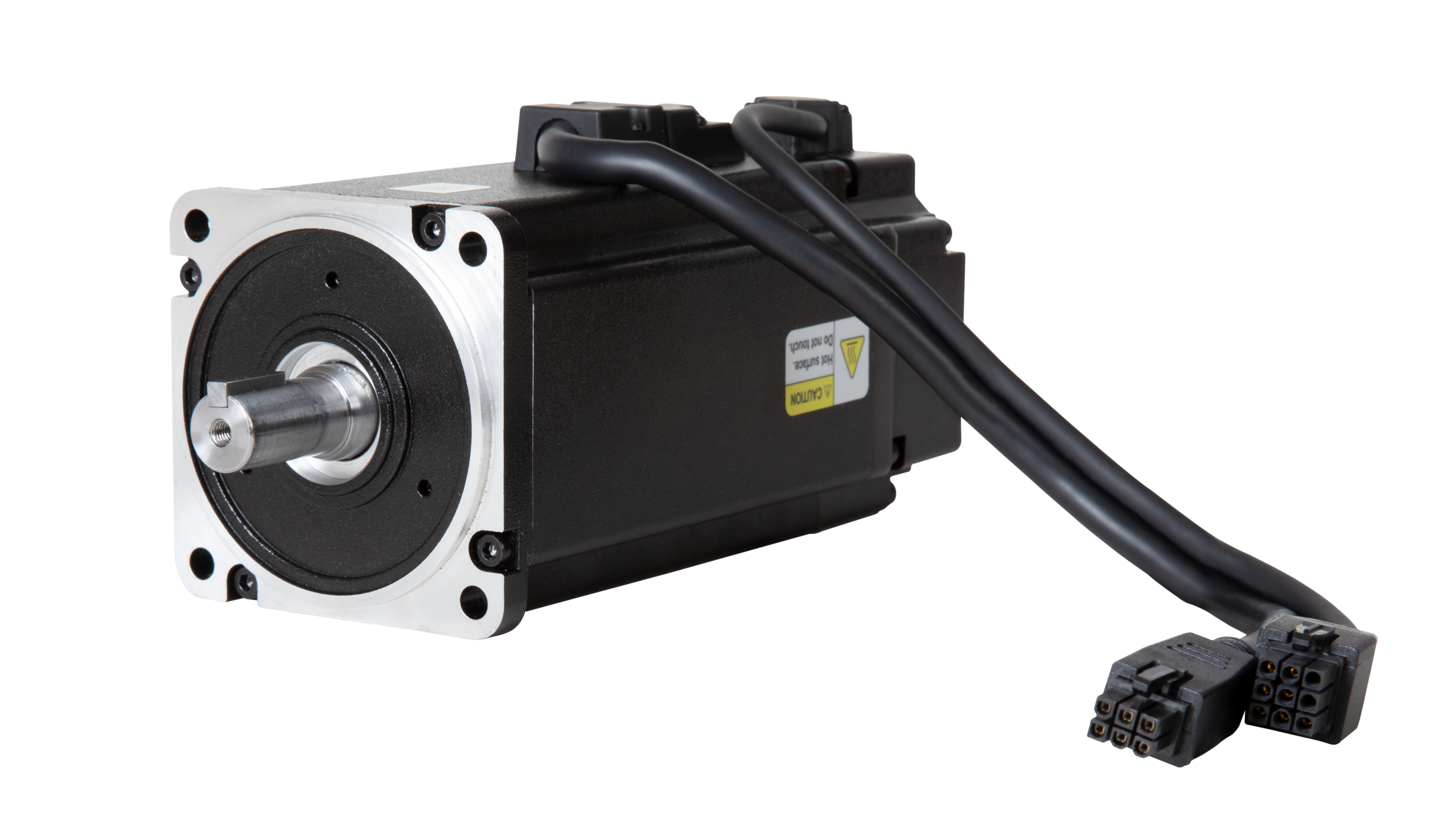
Kinetix TLP Multi-purpose Compact Servo Motors
With an excellent power-to-size ratio, these innovative compact servo motors deliver exceptional performance while minimizing space requirements.
Kinetix TL and TLY Compact Servo Motors
These low-inertia, high-performance compact servo motors are designed to optimize your low-power industrial applications.
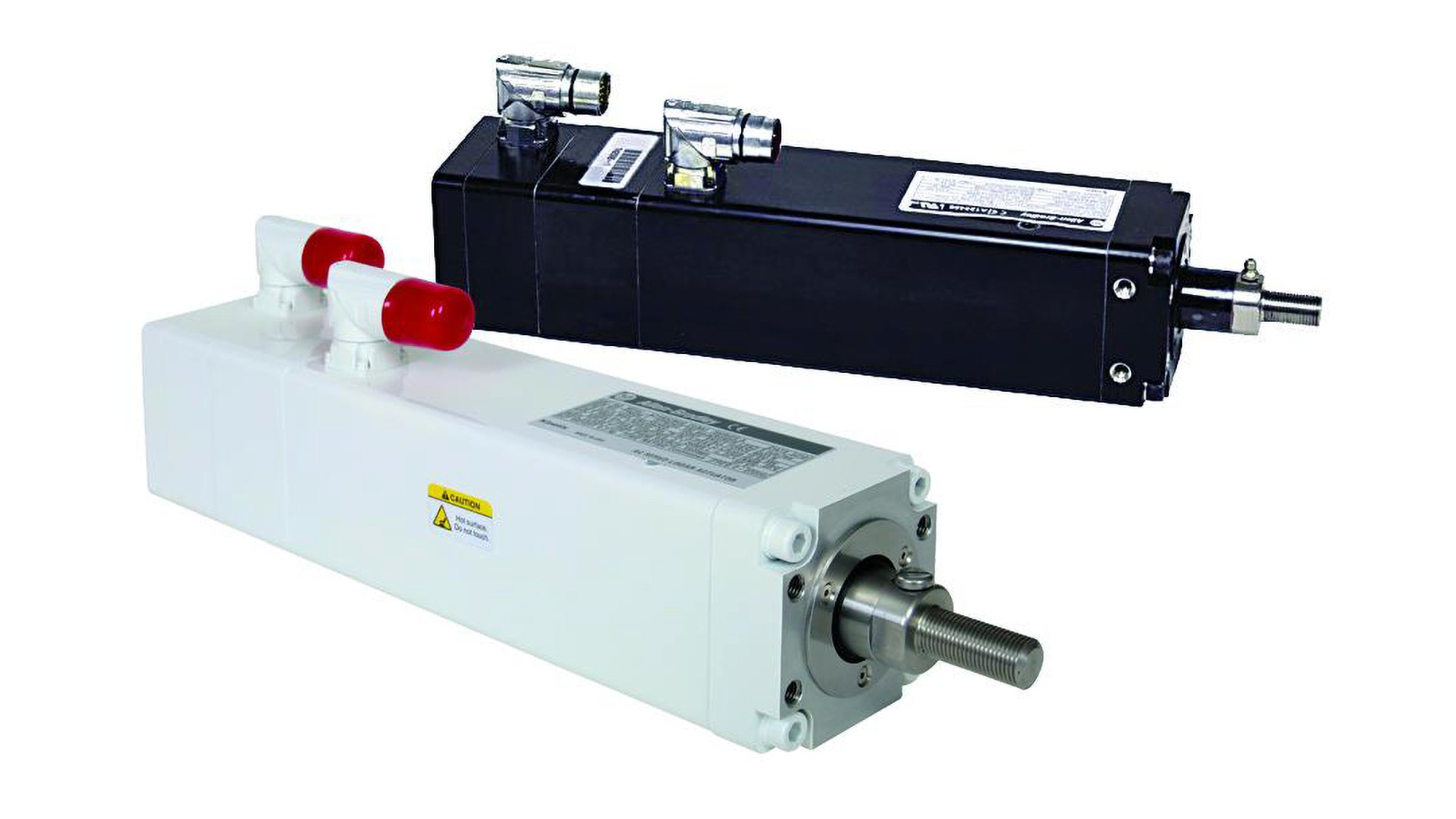
Kinetix VPF Food-grade Servo Motors
These food-grade servo motors provide exceptional performance and durability, allowing you to meet hygienic standards while maximizing productivity.
Kinetix MPF Food-grade Servo Motors
Elevate your operations by combining high-efficiency, high-torque motor capability with features specifically designed for food and beverage applications.
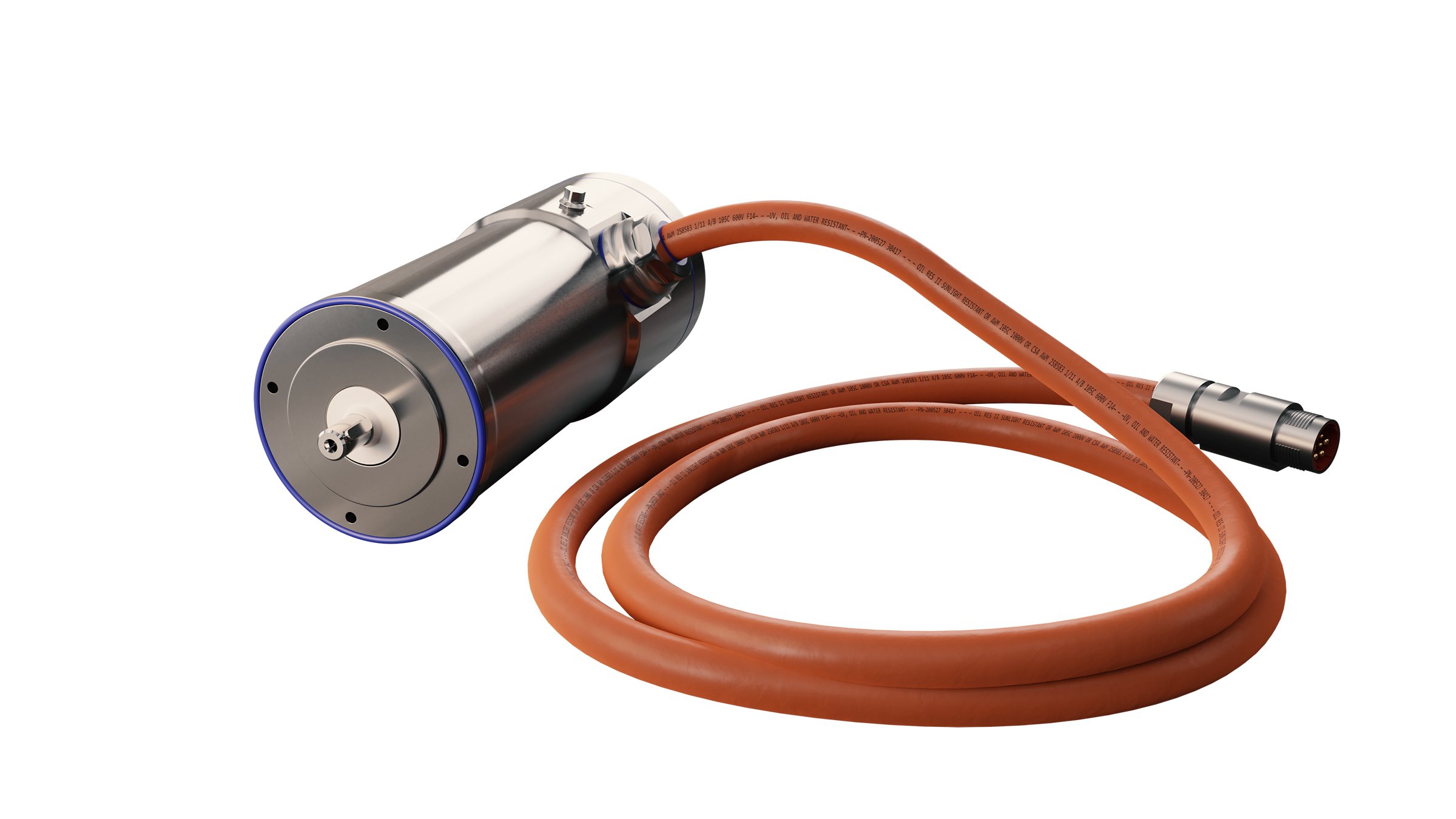
Kinetix VPH Hygienic Servo Motors
These hygienic servo motors feature IP69K ratings and are designed with to operate in harsh environments and handle pressure washdown cleaning.
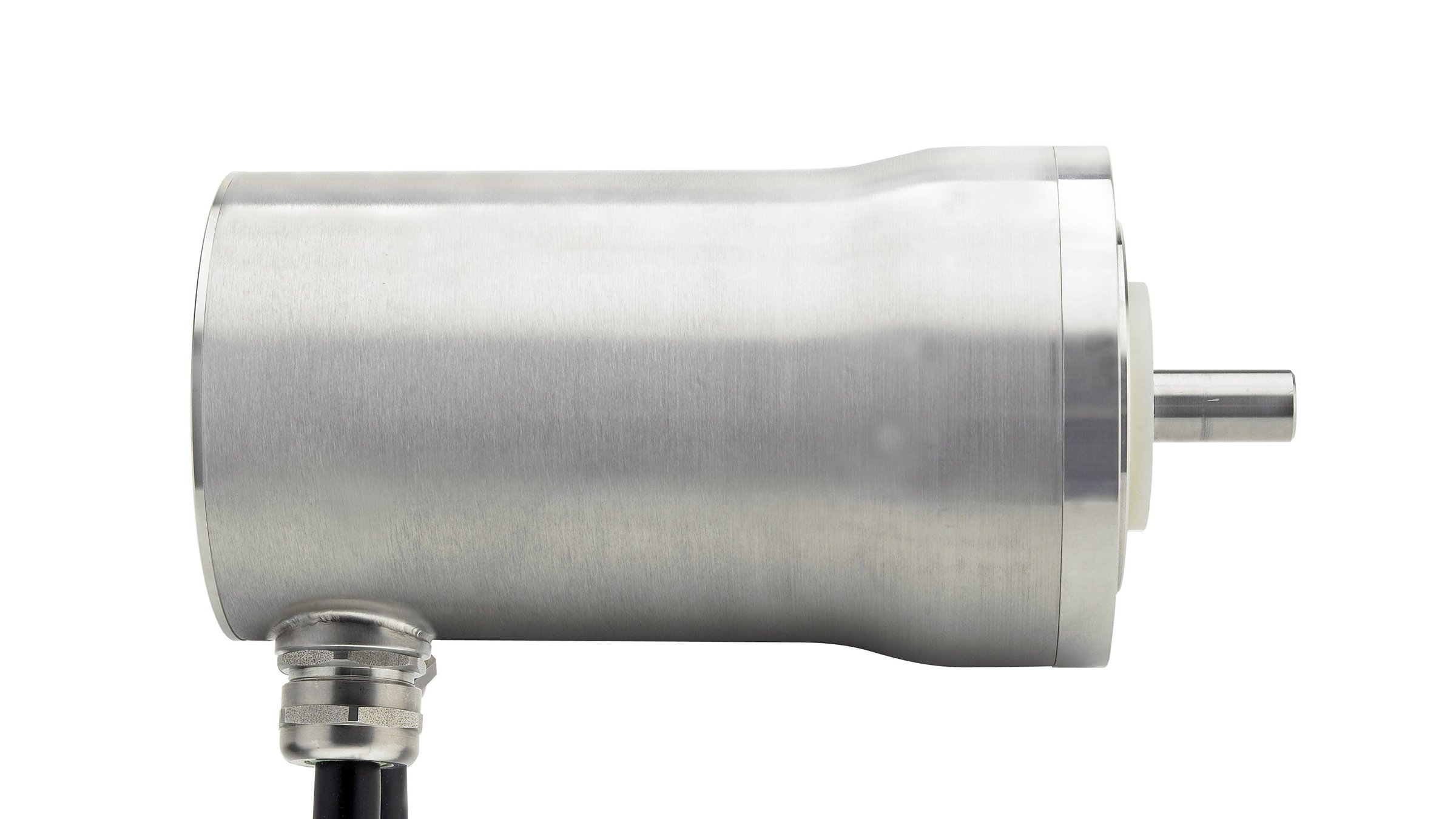
Kinetix MPS Stainless-steel Servo Motors
Use these motors to meet your manufacturing goals even in high pressure or highly caustic wash-down environments.
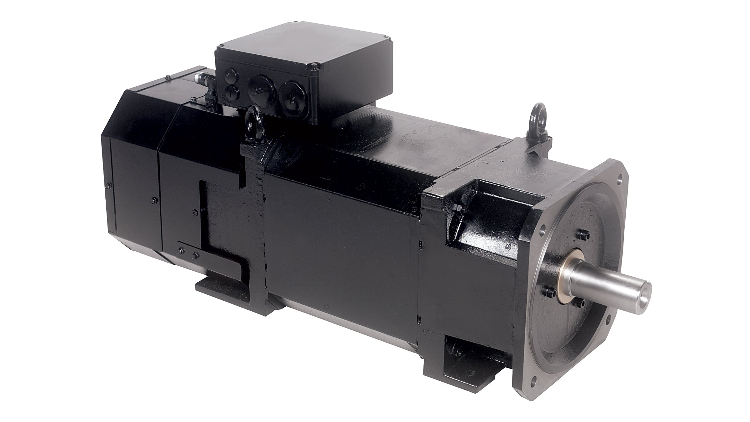
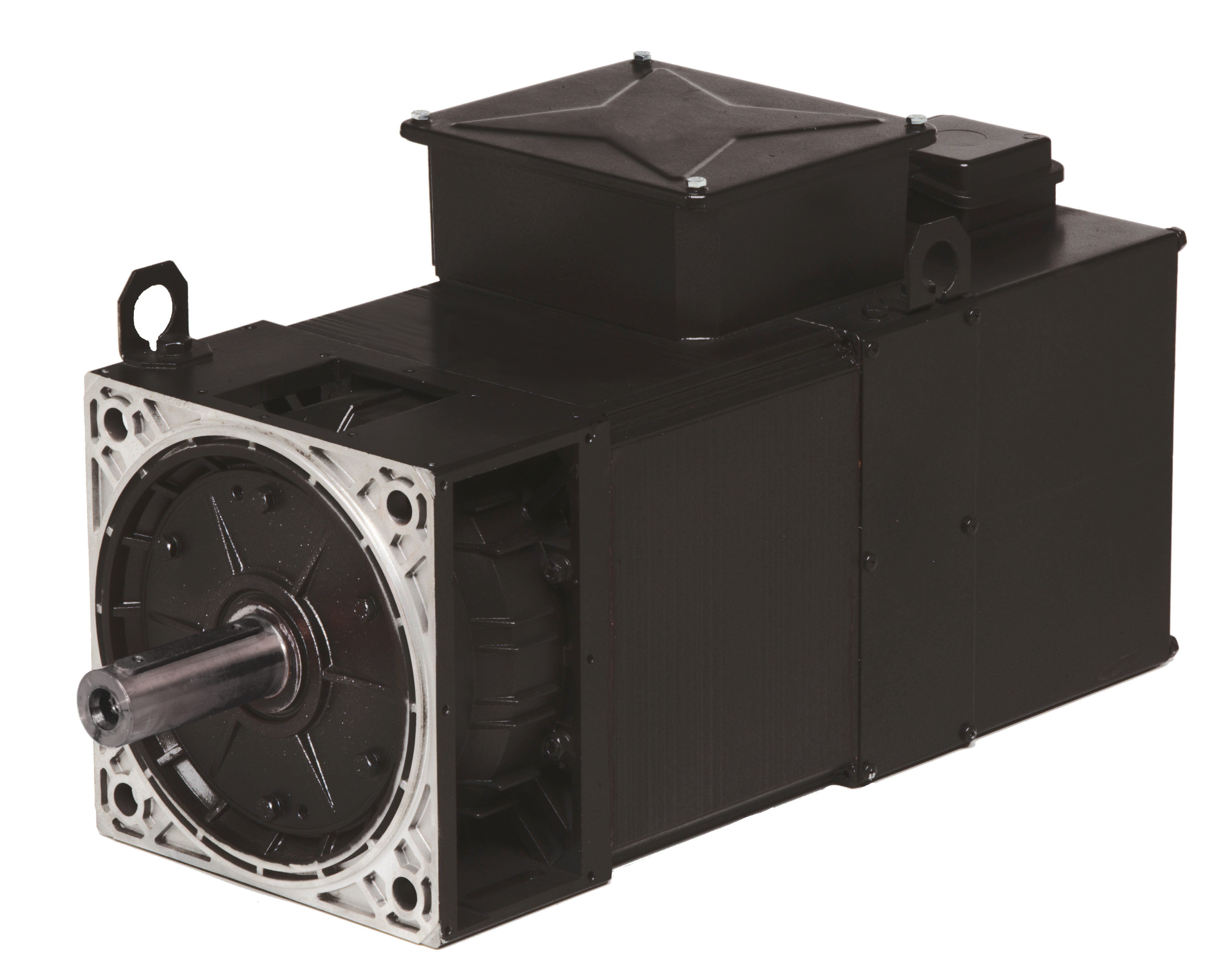
Kinetix MMA Asynchronous Main Motors
Our Kinetix MMA Asynchronous Main Motors enable you to get more from a wide range heavy-duty applications that require high power and torque output.
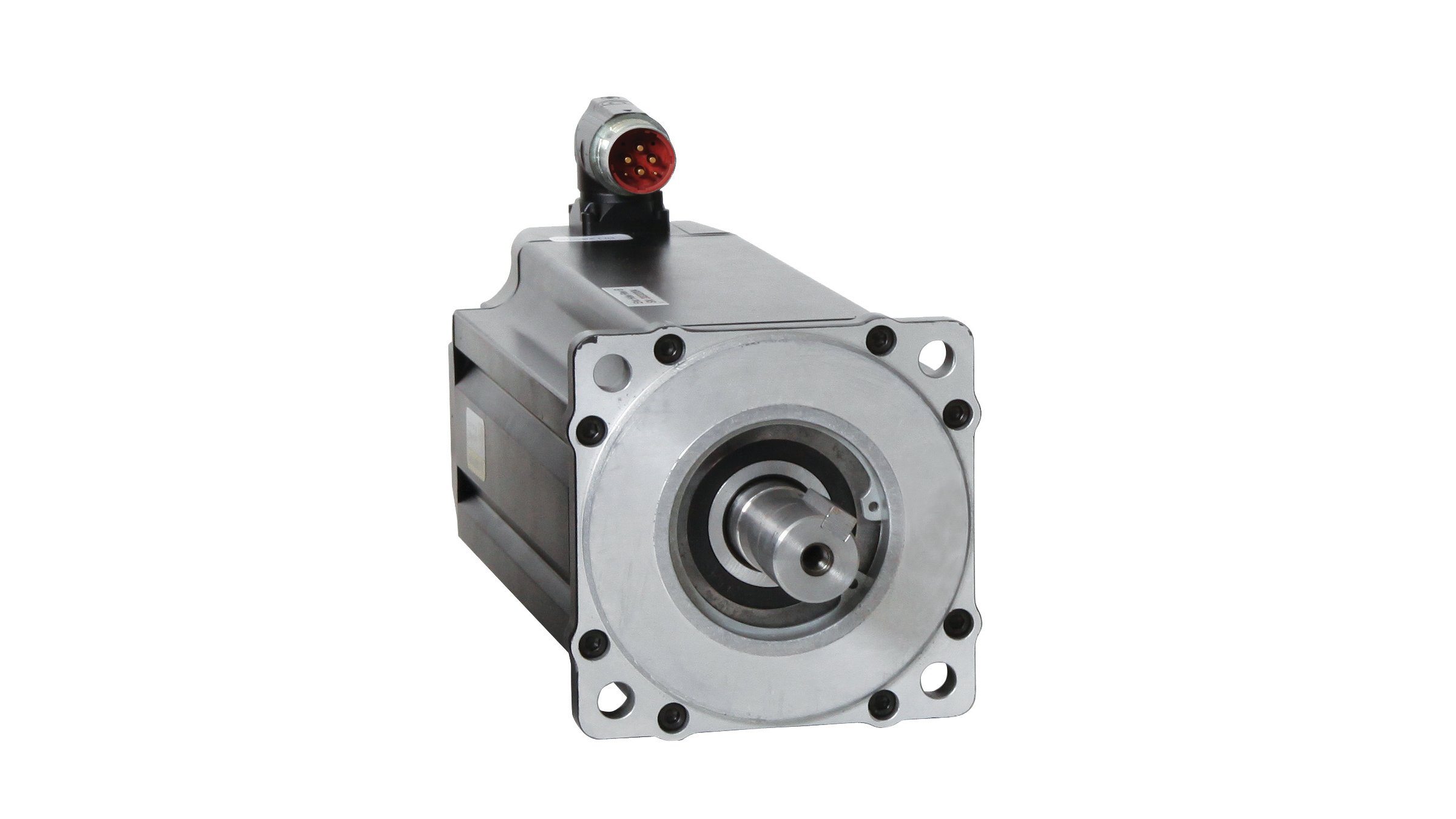
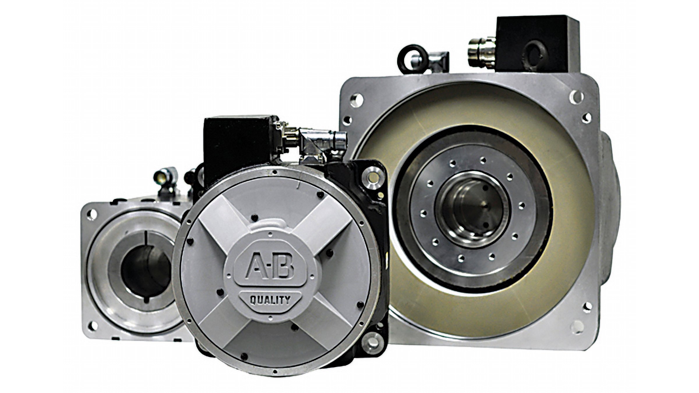
Kinetix RDB Direct-drive Servo Motors
Our direct-drive servo motors enable motion solutions that are simpler, more responsive and operate with better energy efficiency.